

Leadless leadframe with an improved die pad for mold locking
- Summary
- Abstract
- Description
- Claims
- Application Information
AI Technical Summary
Benefits of technology
Problems solved by technology
Method used
Image

Examples
first embodiment
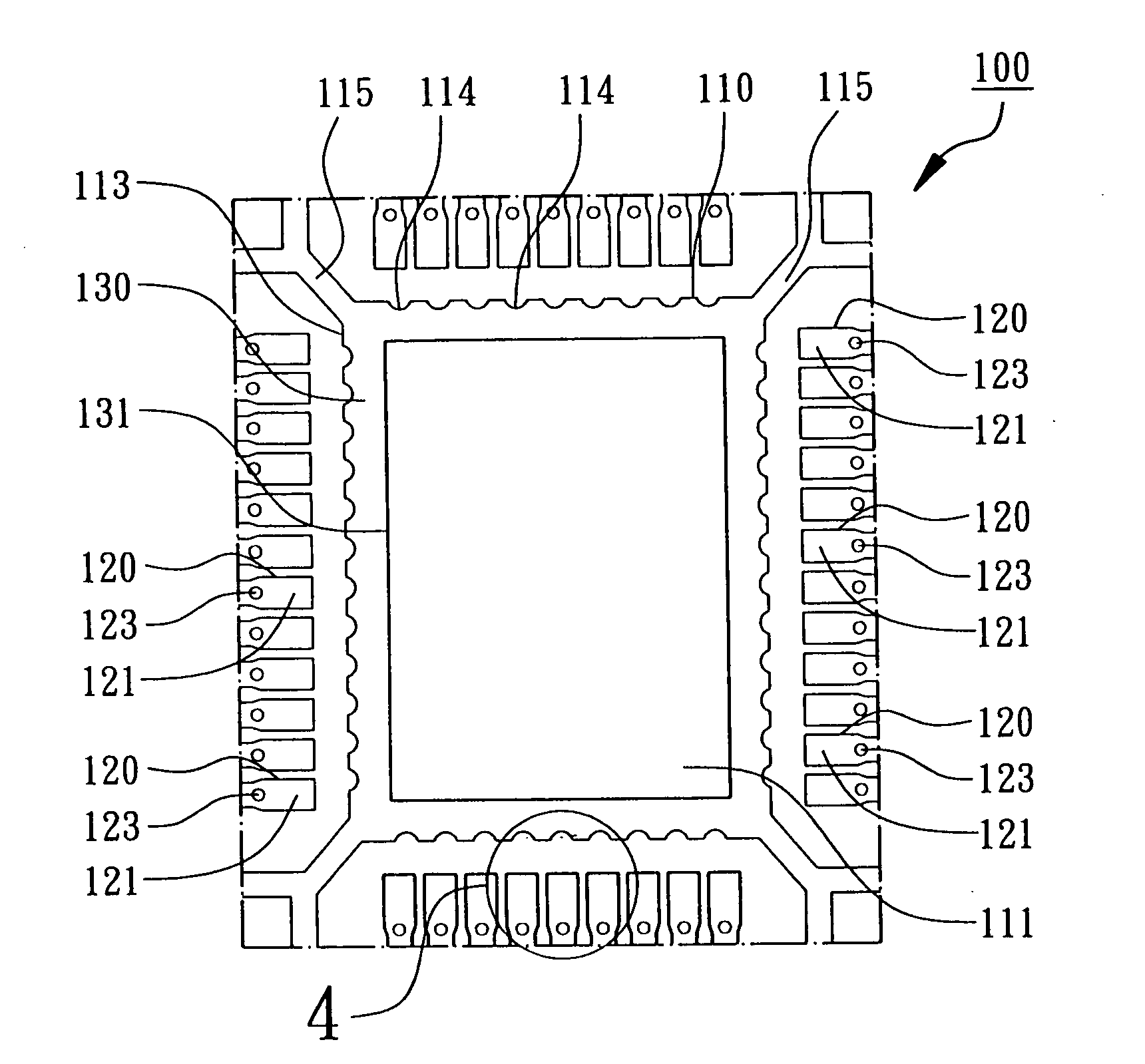
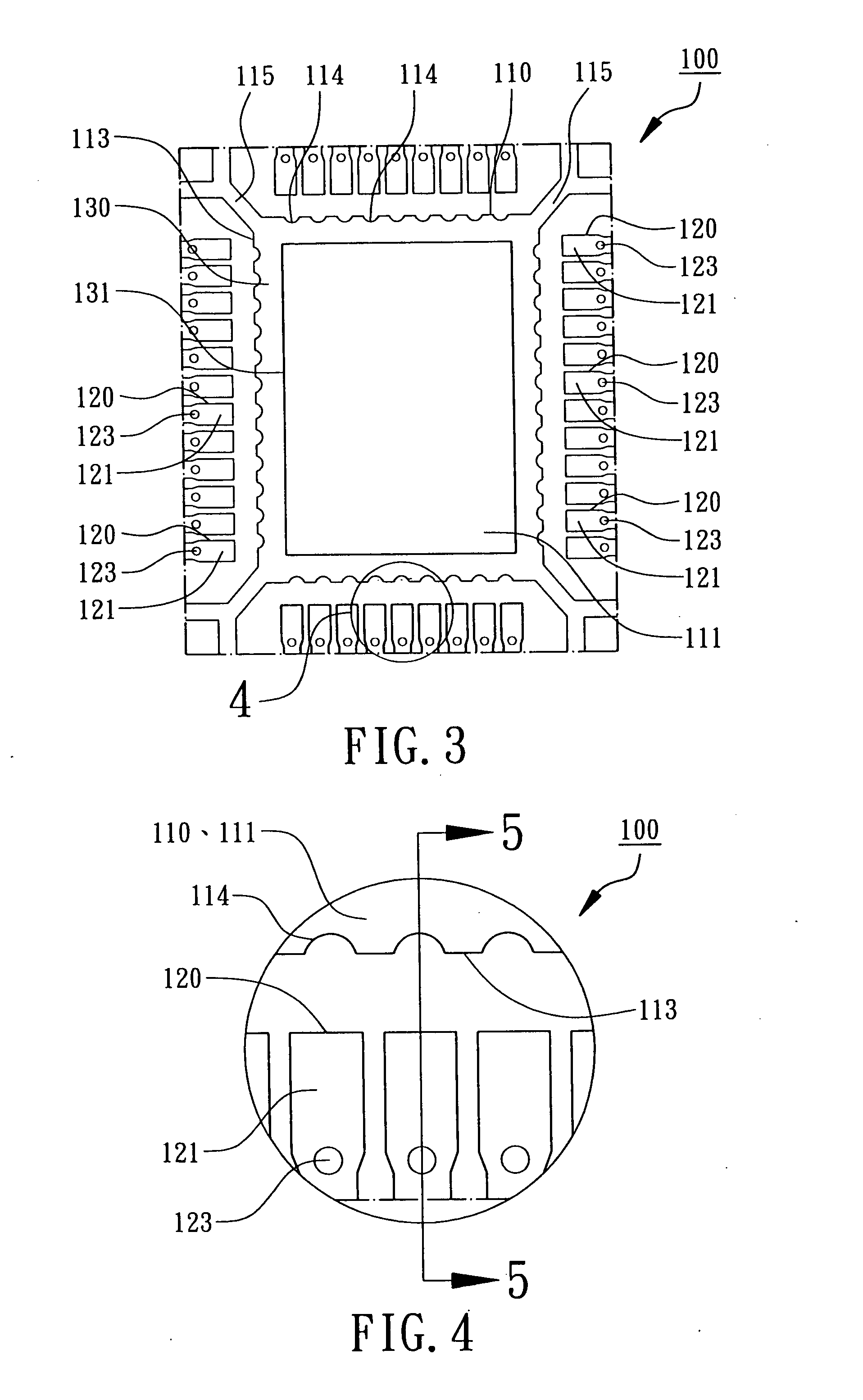
[0019] According to the present invention, a leadless leadframe 100 with an improved die pad for mold locking is shown in FIGS. 3, 4, and 5. The leadframe 100 in each packaging unit comprises a die pad 110 and a plurality of leads 120. The die pad 110 has an upper surface 111, a lower surface 112 and at least a sidewall 113. The sidewall 113 is located between the upper surface 111 and the lower surface 112, as shown in FIG. 5. The sidewall 113 can be vertical or oblique. The height of the sidewall 113 can be equal to or smaller than the thickness of the die pad 110. As shown in FIG. 6, the upper surface 111 of the die pad 110 is configured for attaching a semiconductor chip 210. The lower surface 112 of the die pad 110 is exposed out of the bottom of a package body 230 for enhancing the capability of heat dissipation and providing an electrical connection of ground, as shown in FIG. 6. The die pad 110 is connected to frame of the leadless leadframe 100 via a plurality of tie bars 1...
third embodiment
[0022] In accordance with the present invention a leadless leadframe with an improved die pad for mold locking is shown in FIGS. 9, 10 and 11. The leadless leadframe 300 in each packaging unit comprises a die pad 310 and a plurality of bonding wires 320. The die pad 310 has an upper surface 311, a lower surface 312, and a sidewall 313. The leads 320 are arranged around the die pad 310. A plurality of indentations 314 are formed on the sidewall 313 of the die pad 310. The indentations 314 are vertical grooves extending from the periphery of the upper surface 311. In this embodiment, the indentations 314 include side semi-vias which are in V-shape, as shown in FIGS. 9 and 11. A half-etching portion 315 is formed at the periphery of the lower surface 312 of the die pad 310 and the periphery of the lower surface of the leads 320, so that the area of the upper surface 311 is larger than the area of the lower surface 312. Thus the indentations 314 may not extend to the lower surface 312 o...
PUM
 Abstract
Description
Claims
Application Information