Semiconductor device including a plurality of circuit element chips and a manufacturing method thereof

a semiconductor device and manufacturing method technology, applied in the direction of semiconductor devices, semiconductor/solid-state device details, electrical apparatus, etc., can solve the problems of difficult to meet the requirements and the yield rate of the manufacturing method of the semiconductor device may decrease, and achieve the effect of high yield rate and high reliability in operation

Active Publication Date: 2005-11-24
LAPIS SEMICON CO LTD
View PDF2 Cites 28 Cited by
  • Summary
  • Abstract
  • Description
  • Claims
  • Application Information

AI Technical Summary

Benefits of technology

[0006] An object of the present invention is to provide a semiconductor device, including a plurality of circuit element chips, which possesses higher reliability in its operation with the miniaturization by the CSP technology realized, and to provide a manufacturing method of the semiconductor device in which the yield rate is higher.

Problems solved by technology

On such an occasion as this, the semiconductor chip may move out of the desired location, and then a yield rate in the manufacturing method of the semiconductor devices may decrease.
Also, the packaging technology of the Patent Document 3 requires complicated processes and a position adjustment of the semiconductor chip with a high degree of accuracy, and then, it is not easy to meet those requirements.

Method used


Image

  • Semiconductor device including a plurality of circuit element chips and a manufacturing method thereof
  • Semiconductor device including a plurality of circuit element chips and a manufacturing method thereof
  • Semiconductor device including a plurality of circuit element chips and a manufacturing method thereof

Examples


Embodiment Construction

[0019] Embodiments of the present invention will be described hereinafter with reference to the accompanying drawings. The drawings used for this description illustrate major characteristic parts of embodiments in order that the present invention will be easily understood. However, the invention is not limited by these drawings.

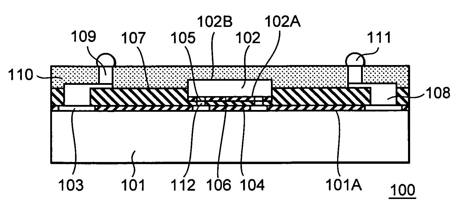
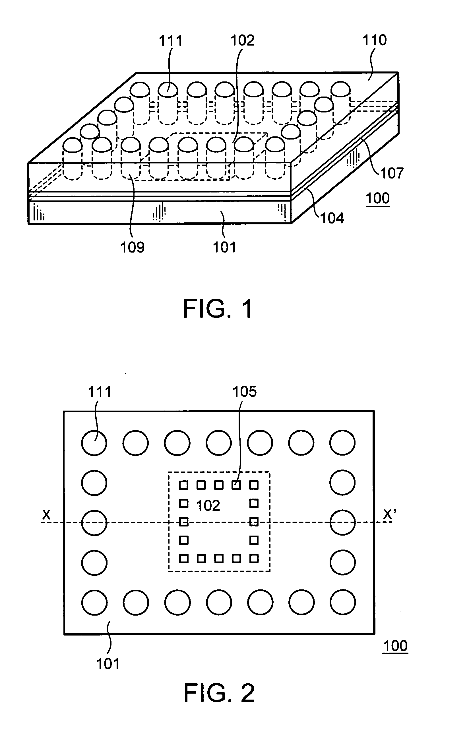
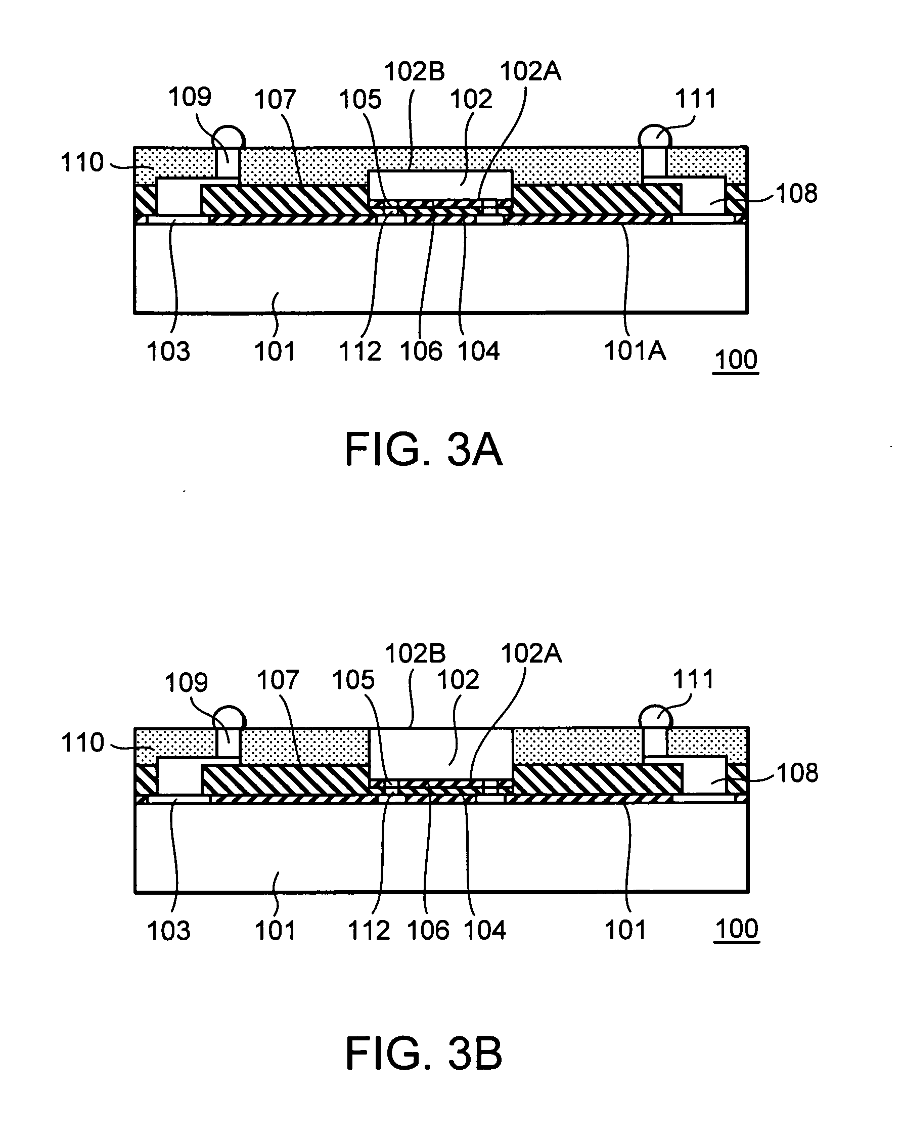
[0020]FIG. 1 is a perspective view of a semiconductor device 100 according to a first preferred embodiment of the present invention. FIG. 2 is a top plan view for describing the semiconductor device 100 in FIG. 1. FIG. 3A is a cross-sectional view for describing the semiconductor device 100 along a dashed-line X-X′ in FIG. 2.

[0021] As shown in FIGS. 1 through 3A, the semiconductor device 100 includes a first circuit element chip 101 and a second circuit element chip 102 which is mounted on the first circuit element chip 101. The first circuit element chip 101 includes a first surface 101A in which a first circuitry has been formed. In this example, for exam...


PUM


Abstract

A semiconductor device includes a first circuit element chip including a first surface on which a plurality of first electrodes are arranged, and a second circuit element chip including a first surface on which a plurality of second electrodes are arranged. The second circuit element chip is mounted on the first circuit element chip. The semiconductor device further includes an insulating film disposed on a side surface of the second circuit element chip and disposed between the first surfaces of the first and second circuit element chips. The semiconductor device still further includes a resin layer covering the second circuit element chip and the insulating film. Also, there is provided a manufacturing method of the semiconductor device which includes forming the insulating film after the second circuit element chip is mounted on the first circuit element chip.

Description

BACKGROUND OF THE INVENTION [0001] 1. Field of the Invention [0002] The present invention relates to a semiconductor device and a manufacturing method of the semiconductor device, in particular, to a semiconductor device which includes a plurality of circuit element chips and a manufacturing method of the semiconductor device. This is a counterpart of and claims priority to Japanese Patent Application No. 2004-148496 filed on May 19, 2004, which is herein incorporated by reference. [0003] 2. Description of the Related Art [0004] Along with a request for miniaturization of electronics devices in recent years, research and development for various methods of high-density packaging of semiconductor devices have been prompted. The methods include a packaging technology of miniaturization of the semiconductor devices per se and a packaging technology of high-density packaging of a plurality of circuit element chips in the semiconductor device. Furthermore, the packaging technology of mini...

Claims


Application Information

Patent Timeline
Patent Type & Authority Applications(United States)
IPC IPC(8): H01L25/18H01L21/48H01L23/48H01L25/065H01L25/07
CPCH01L23/3114H01L25/0657H01L25/16H01L2224/16H01L2225/06513H01L2225/06524H01L2224/16145H01L2225/06586H01L2924/01078H01L2924/01079H01L2924/19041H01L2924/19104H01L2225/06541H01L24/05H01L24/13H01L24/16H01L24/17H01L2224/02377H01L2224/04105H01L2224/05001H01L2224/05008H01L2224/05022H01L2224/05024H01L2224/05147H01L2224/05155H01L2224/05166H01L2224/05171H01L2224/05184H01L2224/05624H01L2224/05644H01L2224/05647H01L2224/06135H01L2224/12105H01L2224/16265H01L2224/1703H01L2224/17051H01L2924/00014
Inventor TERUI, MAKOTO
Owner LAPIS SEMICON CO LTD
Why Eureka
Try Eureka