

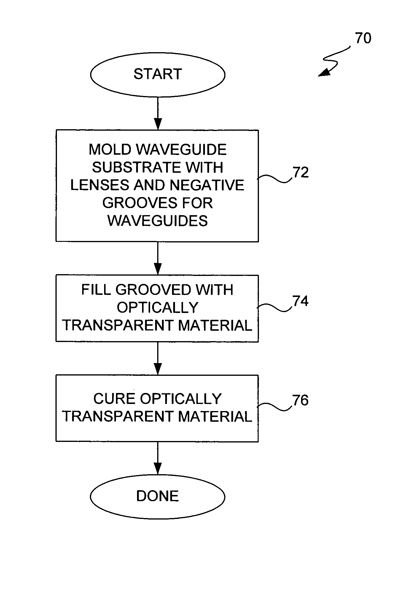
Apparatus and method for a molded waveguide for use with touch screen displays
a touch screen display and waveguide technology, applied in the field of light generation and reception for touch screen displays, can solve the problems of reducing the life of the battery of the device, obscuring the viewing of the underlying display, and affecting the appearance of the display, so as to achieve the effect of simple production and low cos
- Summary
- Abstract
- Description
- Claims
- Application Information
AI Technical Summary
Benefits of technology
Problems solved by technology
Method used
Image

Examples
Embodiment Construction
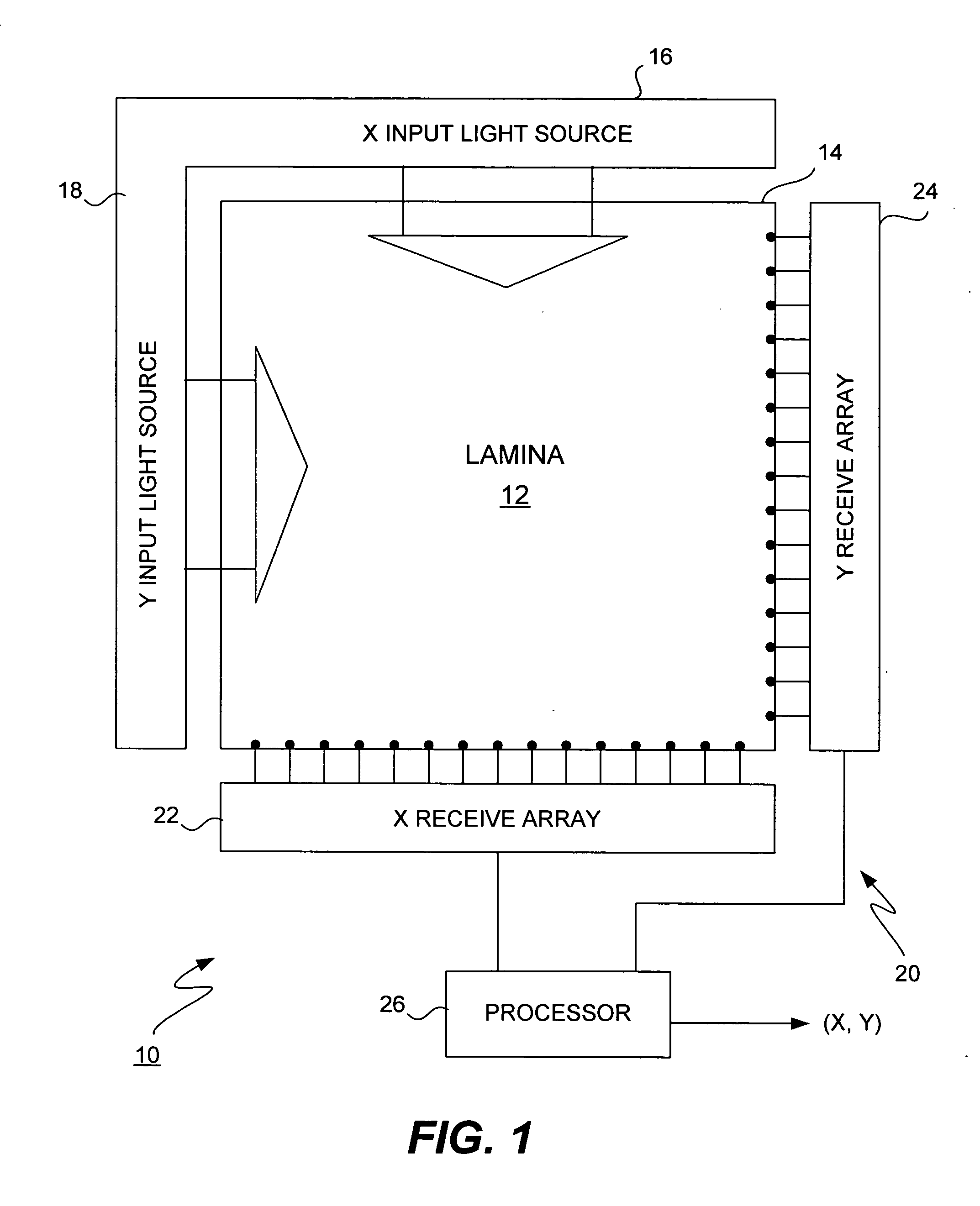
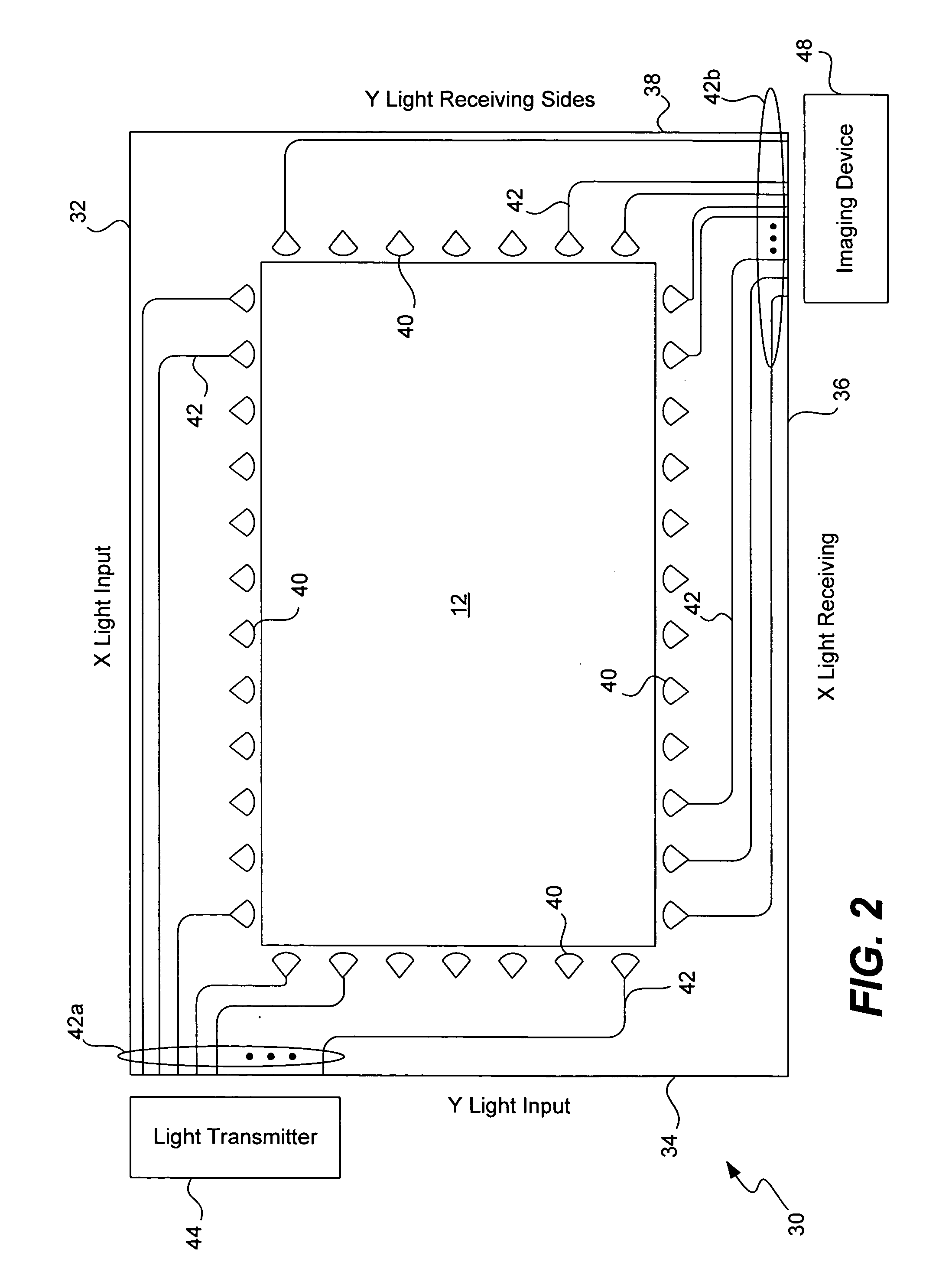
[0019] Referring to FIG. 1, a touch screen data input device is shown. The data input device 10 defines a continuous sheet or “lamina”12 of light in the free space adjacent to a touch screen 14. The lamina 12 of light is created by an X and Y input light sources 16 and 18 respectively. An optical position detection device 20, optically coupled to the lamina of light, is provided to detect data entries to the input device by determining the location of interrupts in the lamina caused when data is entered to the input device. The optical position detection device 20 includes an X receive array 22, a Y receive array 24 and a processor 26. During operation, a user makes a data entry to the device 10 by touching the screen 14 using an input device, such as a finger, pen or stylus. During the act of touching the screen, the lamina 12 of light in the free space adjacent the screen is interrupted. The X receive array 22 and Y receive array 24 of the optical position detection device 20 dete...
PUM
| Property | Measurement | Unit |
|---|---|---|
| diameter | aaaaa | aaaaa |
| depth | aaaaa | aaaaa |
| depth | aaaaa | aaaaa |
Abstract
Description
Claims
Application Information