Multilayer electronic component

Active Publication Date: 2005-12-15
TDK CORPARATION
View PDF5 Cites 11 Cited by
  • Summary
  • Abstract
  • Description
  • Claims
  • Application Information

AI Technical Summary

Benefits of technology

[0013] Preferably, the plurality of first connection regions are provided in the first matrix layer so as to hold the first electrode forming region therebetween, whereas the plurality of second connection regions are provided in the second matrix layer so as to hold the second electrode forming region therebetween at a position different from the first connection regions. When a voltage is applied between the first and second electrodes in this case, the electric field occurring between the electrodes spreads substantially uniformly from the end portion side of the electrodes toward the center thereof. As a consequence, the action of enhancing the uniformity in the electric field distribution can be exhibited effectively.
[0014] Preferably, a first connecting pattern electrically connected to the second through hole electrode is formed on the surface of each first connection region in the first matrix layer, whereas a second connecting pattern electrically connected to the first through hole electrode is formed on the surface of each second connection region in the second matrix layer. This makes it possible to connect a number of first electrodes to each other easily and reliably by way of a plurality of first through hole electrodes and second connecting patterns. Also, a number of second electrodes can be connected to each other easily and reliably by way of a plurality of second through hole electrodes and first connecting patterns. Therefore, even when the number of matrix layers is large, the reliability concerning the connection of inner electrodes can be improved.
[0015] Preferably, the first electrode forming region and first connection regions are formed on the inside of a periphery of the first matrix layer, whereas the second electrode forming region and second connection regions are formed on the inside of a periphery of the second matrix layer. This keeps the inner electrodes from being exposed to the peripheries of the matrix layers. Therefore, in the case where the multilayer electronic component is used as a multilayer piezoelectric element, cracks can be prevented from occurring at interfaces between the matrix layers and inner electrodes even when the multilayer piezoelectric element is continuously driven (displaced). This can also prevent metals and metal ions from migrating because of the moisture attached to side faces of the multilayer p

Problems solved by technology

Therefore, when a voltage is applied between a positive inner electrode and a negative inner electrode, there is a possibility of biasing the distribution of current flowing through the inner electrodes, thereby yielding an uneven electric field distribution between the inner electro

Method used


Image

  • Multilayer electronic component
  • Multilayer electronic component
  • Multilayer electronic component

Examples


Embodiment Construction

[0025] In the following, preferred embodiments of the present invention will be explained in detail with reference to the accompanying drawings. In the explanation, constituents identical to each other or those having functions identical to each other will be referred to with numerals identical to each other without repeating their overlapping descriptions.

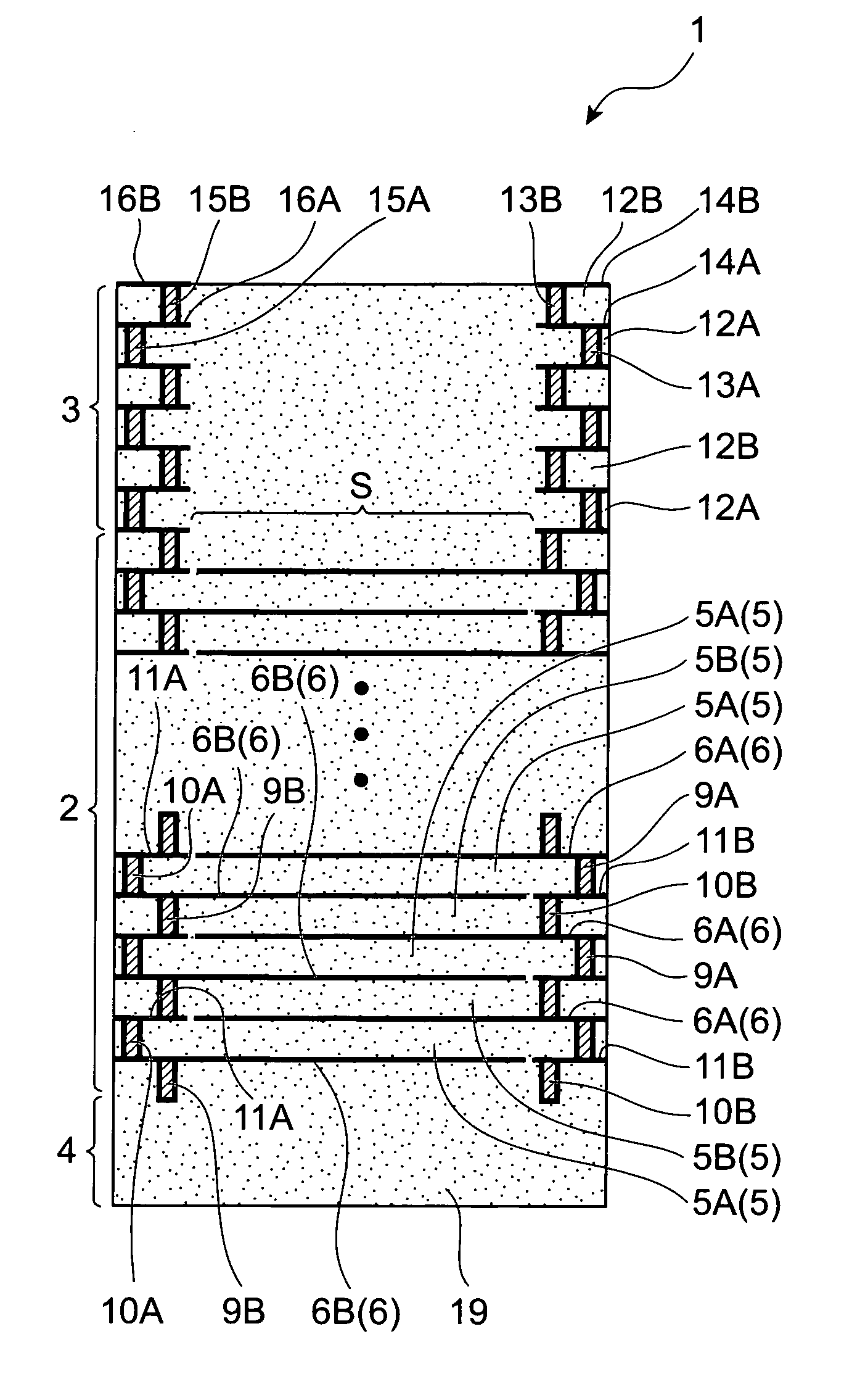
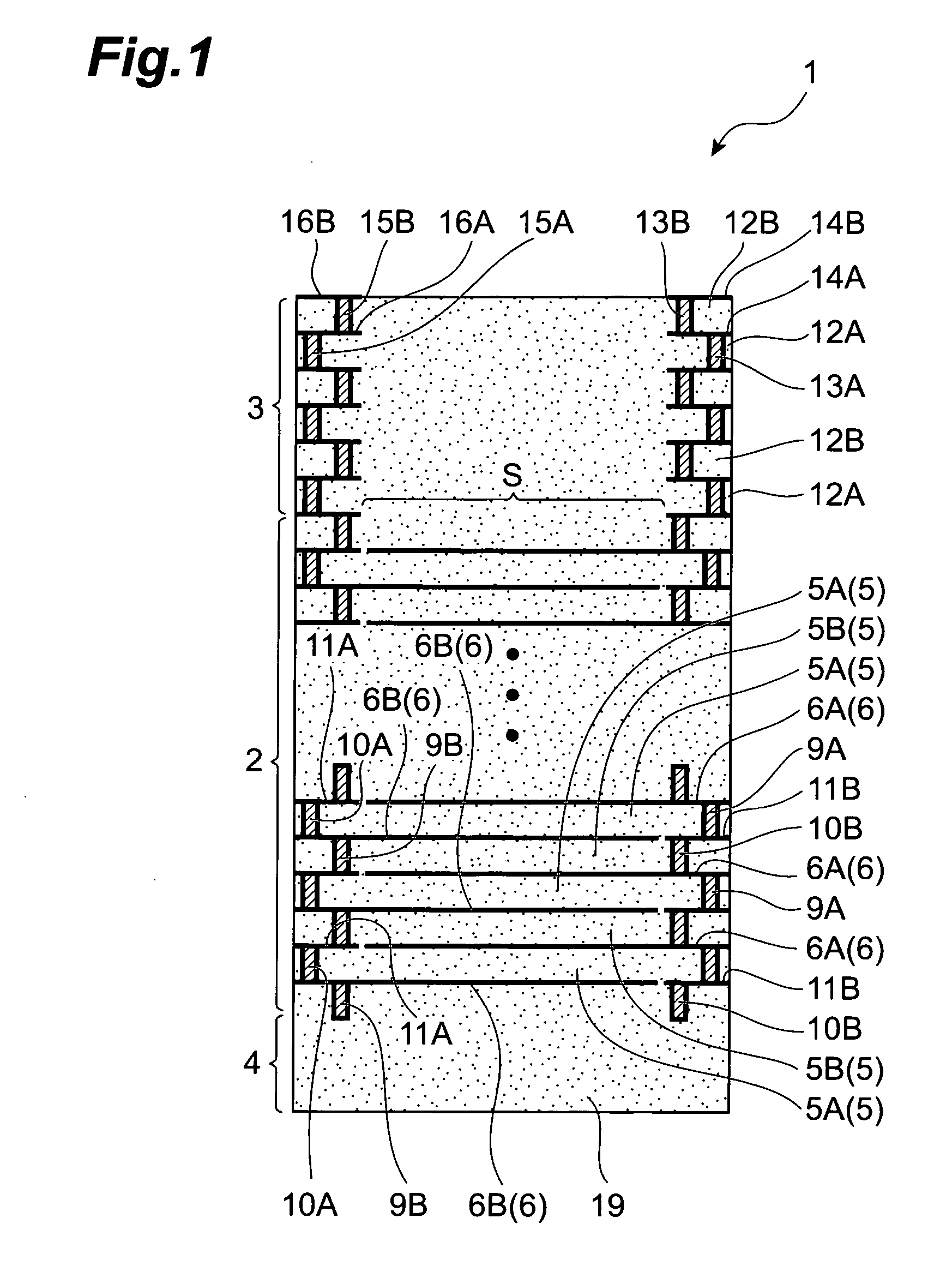
[0026]FIG. 1 is a vertical sectional view showing one embodiment of the multilayer electronic component in accordance with the present invention. In this drawing, the multilayer electronic component in accordance with this embodiment is a multilayer piezoelectric element shaped like a quadratic prism. The multilayer piezoelectric element 1 comprises a piezoelectric element main part 2, an upper lid part 3 disposed on the upper side of the piezoelectric element main part 2, and a lower lid part 4 disposed on the lower side of the piezoelectric element main part 2.

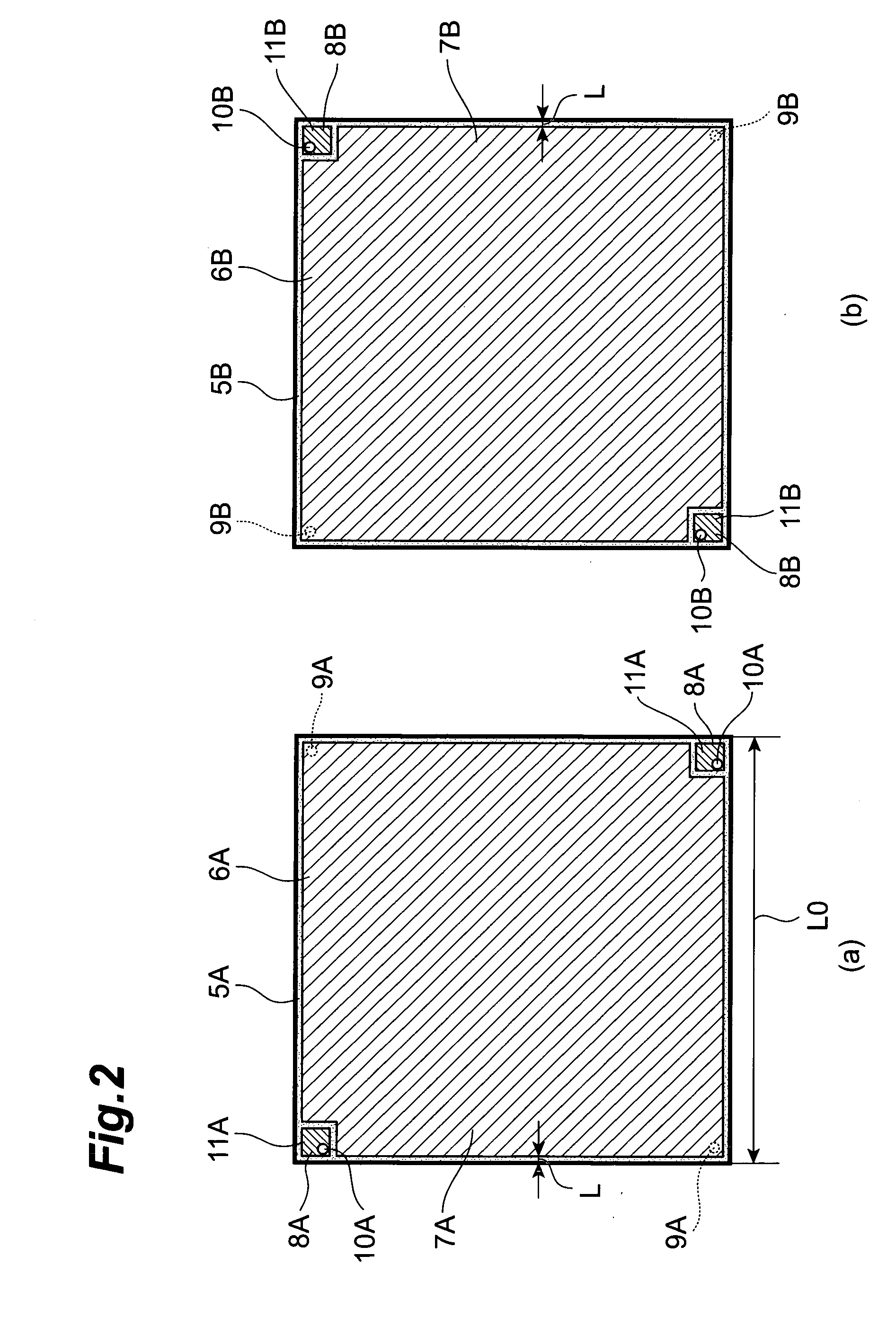
[0027] The piezoelectric element main part 2 is constructed by alte...


PUM


Abstract

A multilayer electronic component comprises a plurality of matrix layers and a plurality of inner electrodes. The matrix layers and inner electrodes are alternately laminated. The plurality of inner electrodes include first electrodes and second electrodes opposing the first electrode while alternating with the matrix layers. Each matrix layer is formed with a plurality of first through hole electrodes for electrically connecting different first electrodes to each other, and a plurality of second through hole electrodes for electrically connecting different second electrodes to each other.

Description

BACKGROUND OF THE INVENTION [0001] 1. Field of the Invention [0002] The present invention relates to a multilayer electronic component. [0003] 2. Related Background Art [0004] Known as an example of conventional multilayer electronic components is a multilayer piezoelectric element disclosed in Japanese Patent Application Laid-Open No. 2000-261055. The multilayer piezoelectric element disclosed in Japanese Patent Application Laid-Open No. 2000-261055 includes a piezoelectric ceramic body formed by laminating a plurality of piezoelectric ceramic green sheets printed with inner electrodes, whereas the piezoelectric ceramic body is formed with two via holes penetrating through the inner electrodes. Conductor leads for electrically connecting the vertically alternating inner electrodes are disposed within the via holes. SUMMARY OF THE INVENTION [0005] In the prior art mentioned above, the inner electrodes of the same polarity alternating with the other layers are connected together with...

Claims


Application Information

Patent Timeline
IPC IPC(8): H01L41/083H05K1/11H01L41/22H01L41/187H01L41/047H01L41/27H01L41/293H01L41/297
CPCH01L41/0474H10N30/874
Inventor SASAKI, SATOSHI
Owner TDK CORPARATION
Why Eureka
Try Eureka