Image display method and image display device

a technology of image display and image, which is applied in the direction of television systems, instruments, color signal processing circuits, etc., can solve the problems of inability to use consumer devices realistically, and the variation in luminance due to the variation in initial light emitted from fluorescent substances cannot be corrected, so as to correct both the variation in initial light emission characteristics and the change therein with time, and display stably the effect of uniform imag

Inactive Publication Date: 2006-01-05
CANON KK
View PDF3 Cites 7 Cited by
  • Summary
  • Abstract
  • Description
  • Claims
  • Application Information

AI Technical Summary

Benefits of technology

[0010] According to the present invention, it is possible to adequately correct both the variation in the initial light emission characteristics and the change therein with time. Therefore, an image display device that stably displays a uniform image can be provided.

Problems solved by technology

In addition, when a change in luminance with time is measured, it is necessary to prepare a dark room and a CCD camera, so this is not realistic for use in a consumer device.
However, the variation in luminance due to the variation in initial light emitted from the fluorescent substances cannot be corrected.

Method used


Image

  • Image display method and image display device
  • Image display method and image display device
  • Image display method and image display device

Examples


first embodiment

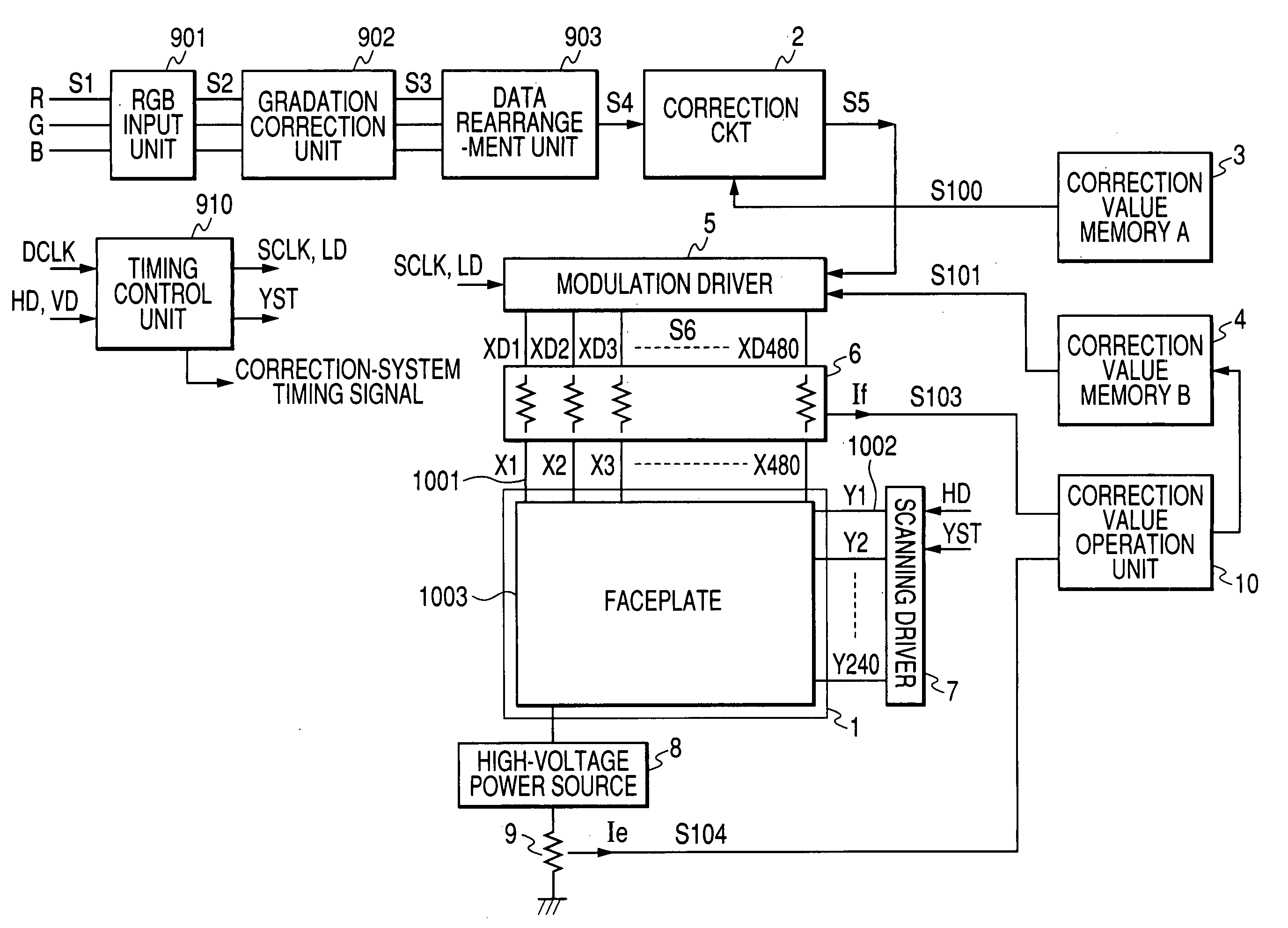
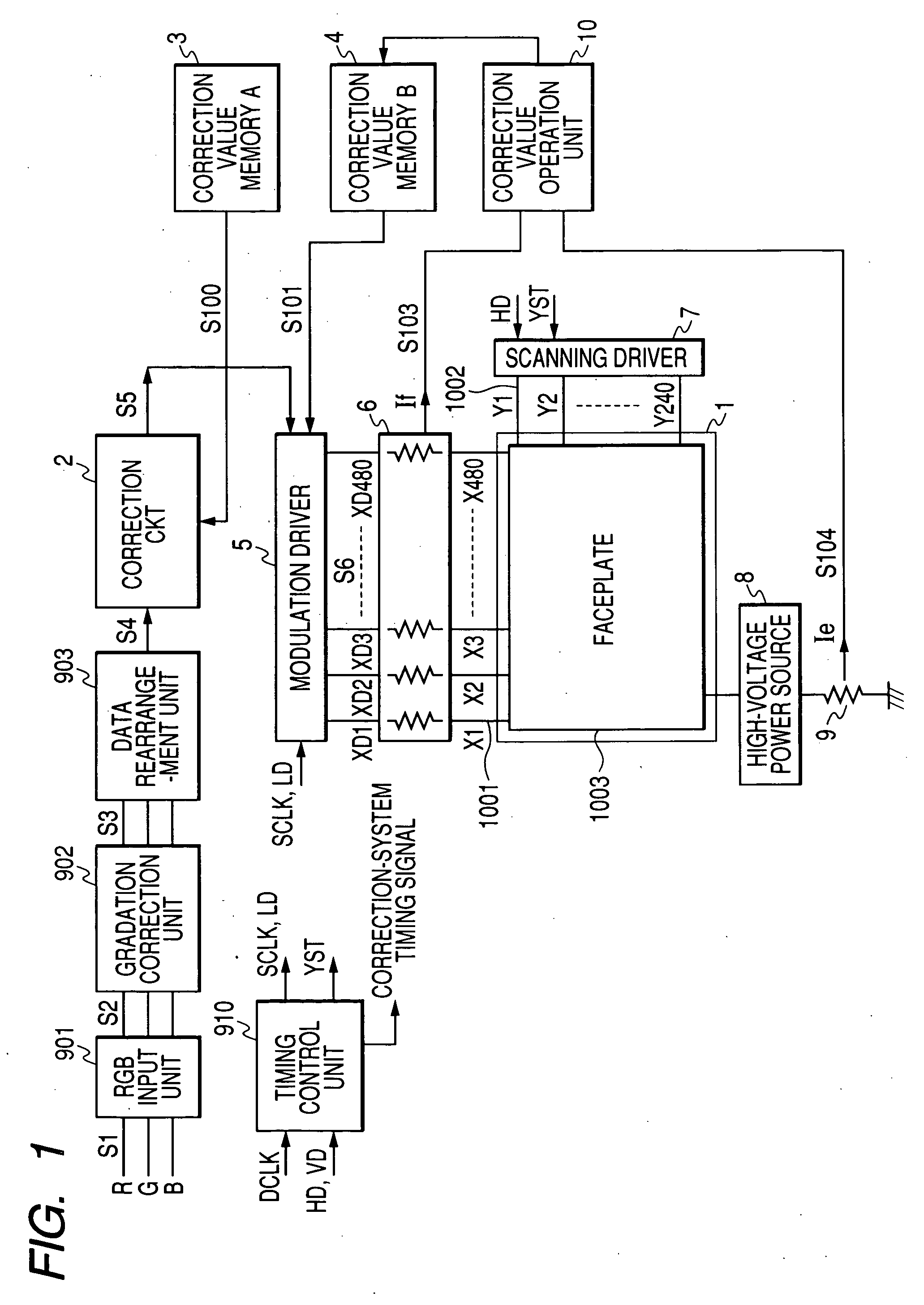
[0053] The first embodiment of the present invention will be described with reference to FIGS. 1 and 2.

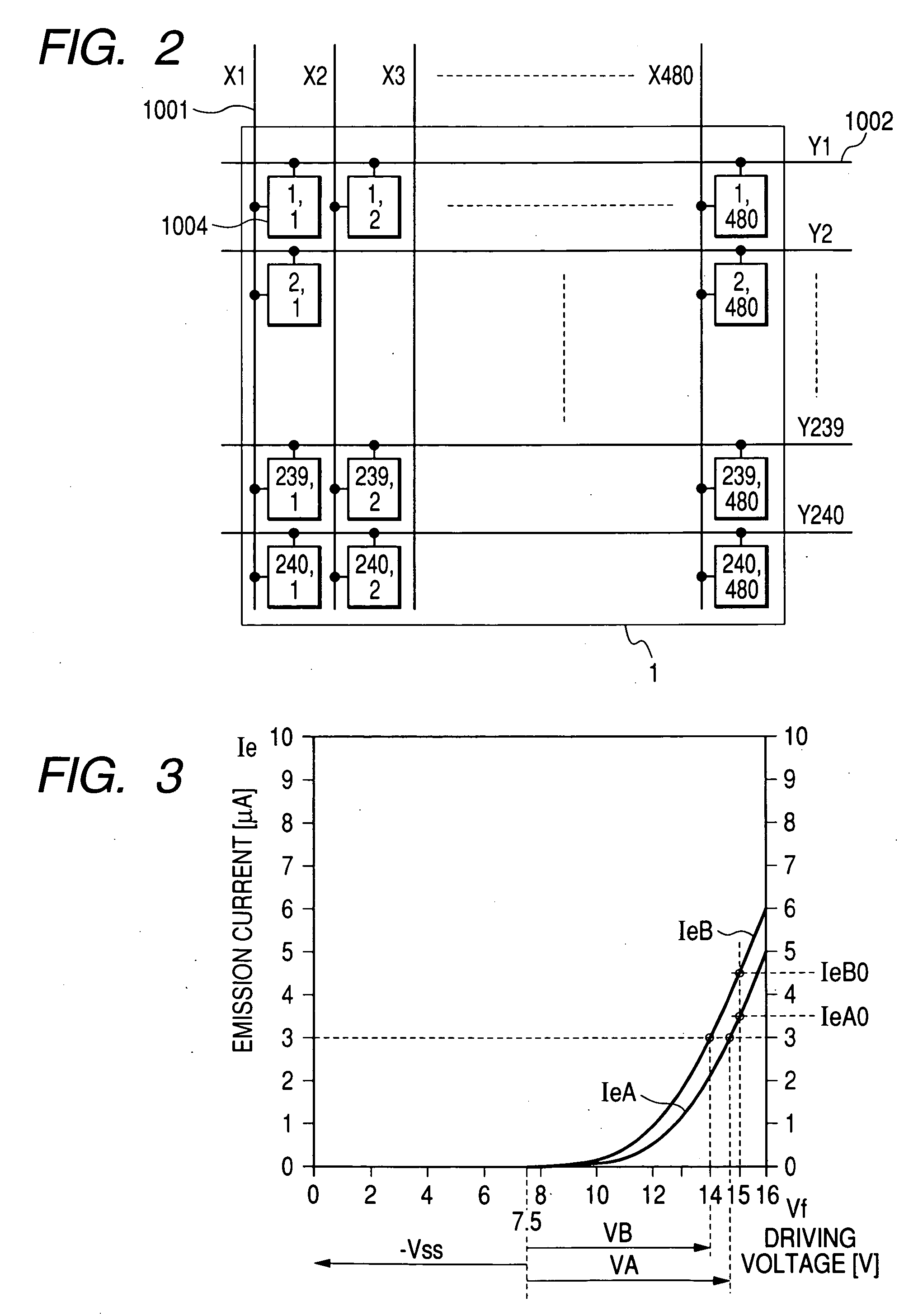
[0054] A matrix panel 1 includes a rear plate having matrix wirings of 240 rows and 480 (160×3 (RGB)) columns and a faceplate 1003 to which a high voltage is applied.

[0055] Scanning wirings 1002 are sequentially selected in response to a horizontal synchronization signal of an inputted image signal. A predetermined selection potential is applied from a scanning driver 7 to each of the scanning wirings for a selection period thereof. Modulation signals corresponding to luminance data for the selected scanning wiring 1002 are applied from a modulation driver 5 to modulation wirings 1001 through an If measurement circuit 6 for the selection period. Such operation for the selection period is performed on each of all the rows, so a screen image is formed after one vertical scanning period is completed.

[0056] In the present embodiment, the number of scanning wirings is set to 240. Whe...

second embodiment

[0100] A fundamental idea of correction according to the second embodiment of the present invention is as follows. (1) With respect to the correction of the variation in emission currents, a PWM pulse width is set to be variable (image data is corrected) and controlled such that emission charge amounts from all electron sources become equal to one another. (2) Even with respect to the correction of the variation in light emitted from the fluorescent substances, the output signal S4 serving as image data which is inputted to the correction circuit 2 is changed into the output signal S5 serving as image data for eliminating the variation in light emission (PWM pulse width is changed). Therefore, the unevenness of display of the matrix panel is preferably corrected.

[0101]FIGS. 8 and 9 are explanatory diagrams showing the second embodiment of the present invention. FIG. 8 is a functional block diagram identical to that of FIG. 1 and thus the descriptions of the functional blocks and th...

third embodiment

[0124]FIG. 15 shows the third embodiment of the present invention.

[0125] In FIG. 15, the descriptions of the same functional blocks as those in the second embodiment shown in FIG. 8 and the like are omitted here.

[0126] The correction circuit 2 corrects the output signal S4 based on the expression (5) to obtain the output signal S5. Therefore, when a new correction value Mi is expressed by the following expression (6):

Mi=(Ki×Ji)  (6)

the following expression (7) can be obtained.

Dout=Din×Mi  (7)

[0127]FIG. 16 shows the correction circuit 2 of the third embodiment. The correction value operation unit 10 calculates the new correction value Mi in advance based on contents of an FP information memory 3b and causes a correction value memory C 3a to store the calculated new correction value Mi. Here, when the correction circuit 2 shown in FIG. 16 is used, the unevenness of light emitted from the image display device can be suitably corrected as in the second embodiment. Note that the co...


PUM


Abstract

Provided is an image display method for an image display device including a plurality of electron emission elements and a fluorescent substance that emits light by electron irradiation from the electron emission elements, the method including: storing a fluorescent substance correction value for correcting variation in the light emitted from the fluorescent substance; continually updating an emission current correction value for correcting variation in an emission current; and driving the image display device based on the fluorescent substance correction value and the updated emission current correction value. According to the method, it is possible to correct both the variation in emission currents and the variation in light emitted from fluorescent substances, and to suppress the unevenness of light emitted in the image display device.

Description

BACKGROUND OF THE INVENTION [0001] 1. Field of the Invention [0002] The present invention relates to an image display device in which a large number of electron emission elements are arranged and electron emission is controlled based on image data and an image display method for the image display device. In particular, the present invention relates to an image display method of adequately correcting both the variation in light emitted from fluorescent substances and the variation in emission currents from the electron emission elements and an image display device operated by the image display method. [0003] 2. Related Background Art [0004] The following technique has been disclosed in Japanese Patent Application Laid-Open No. 2001-350442 (hereinafter called document 1). According to the technique, in order to realize display of a field emission display (FED) that eliminates non-uniformity in illumination with respect to both initial characteristics and a change with time, luminance ...

Claims


Application Information

Patent Timeline
Patent Type & Authority Applications(United States)
IPC IPC(8): H01J11/00H04N5/70G09G3/20G09G3/22H04N5/68
CPCG09G3/2014H04N17/04G09G3/22G09G2310/027G09G2320/0285G09G2320/029G09G2320/043G09G2330/12G09G2360/147H01J31/127H04N5/44H04N9/30H04N9/69H04N9/73H04N17/02G09G3/2081
Inventor ABE, NAOTOSAITO, HIROSHIIKEDA, TAKESHI
Owner CANON KK
Why Eureka
Try Eureka