Semiconductor memory device

Inactive Publication Date: 2006-01-05
POLARIS INNOVATIONS
View PDF7 Cites 4 Cited by
  • Summary
  • Abstract
  • Description
  • Claims
  • Application Information

AI Technical Summary

Benefits of technology

[0024] In one embodiment, the semiconductor memory device furthermore comprises at least one frequency divider, which is provided between the ring oscillator and the measurement terminal, for the purpose of reducing the frequency of the ring oscillator.
[0025] Providing the frequency divider may make it possible to reduce the frequency of the ring oscillator, so that the frequency output at the measurement terminal is lower. Consequently, in one embodiment, it not necessary to provide an external test device that can measure very high-frequency signals. Consequently, it is possible to use a conventional test device.
[0026] In one embodiment, the frequency divider further preferably comprises local frequency divider units that are in each case assigned to a test circuit, for the purpose of reducing the frequency output by the test circuit, and at least one global frequency divider unit, to which a plurality of local frequency divider units are in signal connection, for the purpose of reducing the frequency reduced by the local frequency divider units.

Problems solved by technology

When a semiconductor memory device is operated or tested at high frequency, e.g. with a clock frequency of more than 500 MHz, however, it becomes increasingly more difficult to check the accuracy of the interface timing since it is necessary to use test devices which can generate such high clock frequencies with a high accuracy and can also measure frequencies with a high accuracy.

Method used


Image

  • Semiconductor memory device
  • Semiconductor memory device
  • Semiconductor memory device

Examples


Embodiment Construction

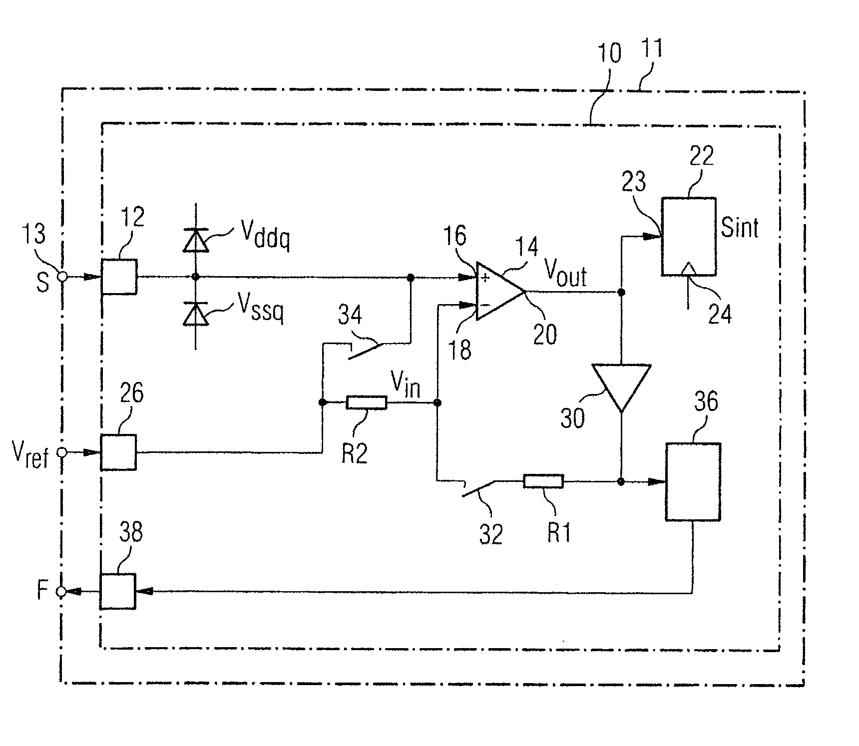
[0042] Testing semiconductor memory devices involves, inter alia, testing whether the so-called interface timing of data signals and data clock signals is within predetermined limits. In particular, the so-called setup time tS and the so-called hold time tH are tested. In this case, the setup time tS is that time period before an edge of a data clock signal in which a data signal which is intended to be read in or out with the edge must have a predetermined value. In this case, the hold time tH is that time period after an edge of a data clock signal in which a data signal which is intended to be read in or out with the edge must have a predetermined value.

[0043] In some cases, the setup time tS and the hold time tH assume very low values particularly in high-frequency operation of the semiconductor memory device at e.g. 500 MHz.

[0044] Furthermore, the temporal ratio of the data signal and the associated data clock signal is of great importance. If, by way of example, the setup ti...


PUM


Abstract

The invention relates to a semiconductor memory device, which can be operated in a normal operating mode and a test mode, comprising: data terminals and data clock terminals; input receivers for processing the signal arriving via the respective terminal, a respective input receiver being assigned to a data terminal and / or data clock terminal; at least one test circuit, a respective test circuit being assigned to an input receiver and the test circuit being designed for determining at least one predetermined property of the assigned input receiver.

Description

CROSS-REFERENCE TO RELATED APPLICATIONS [0001] This application claims foreign priority benefits under 35 U.S.C. §119 to co-pending German patent application number DE 10 2004 030 053.4, filed 22 Jun. 2004. This related patent application is herein incorporated by reference in its entirety. BACKGROUND OF THE INVENTION [0002] 1. Field of the Invention [0003] The invention relates to a semiconductor memory device. [0004] 2. Description of the Related Art [0005] A semiconductor memory device in accordance with the prior art will be described with reference to FIG. 2. FIG. 2 shows a schematic partial view of a packaged semiconductor memory device. [0006] An incoming data signal DQ is transferred via a pin 1 on the package to the pad 2 of the semiconductor memory device 3. An input receiver 4 provided on the semiconductor memory device 3 amplifies the incoming signal and outputs this to a flip-flop 5. A similar construction is provided for the data clock signals DQS in the semiconductor ...

Claims


Application Information

Patent Timeline
IPC IPC(8): G11C8/02G11C29/00G11C29/48
CPCG11C29/48G11C29/1201
Inventor SPIRKL, WOLFGANG
Owner POLARIS INNOVATIONS
Why Eureka
Try Eureka