Metal oxide semiconductor (MOS) varactor

Inactive Publication Date: 2006-01-12
REALTEK SEMICON CORP
View PDF2 Cites 72 Cited by
  • Summary
  • Abstract
  • Description
  • Claims
  • Application Information

AI Technical Summary

Benefits of technology

[0008] It is therefore an object of the invention to provide a varactor, which c

Problems solved by technology

Therefore, the tuning range of the MOS varactor structure can be only increased by reducing the oxide layer thickness or well concentration, for example, as disclosed in Chapter 7, “Physics of semiconductor devices” second edition,

Method used


Image

  • Metal oxide semiconductor (MOS) varactor
  • Metal oxide semiconductor (MOS) varactor
  • Metal oxide semiconductor (MOS) varactor

Examples


Embodiment Construction

[0018] As mentioned in the prior art, the tuning range of the MOS varactor can be only increased by reducing the oxide layer thickness or the well concentration. However, the oxide layer thickness has physical limitation and every semiconductor process has constant oxide layer thickness, which cannot be changed casually, and reducing well concentration means changing process. Therefore, the invention provides a structure of a MOS varactor, which can be manufactured by the available process, for example, the TSMC 0.18 um RF process.

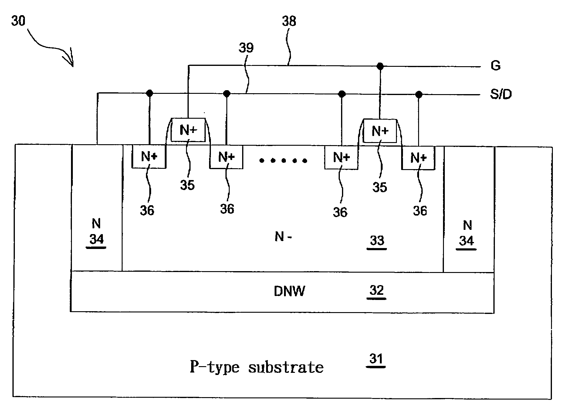
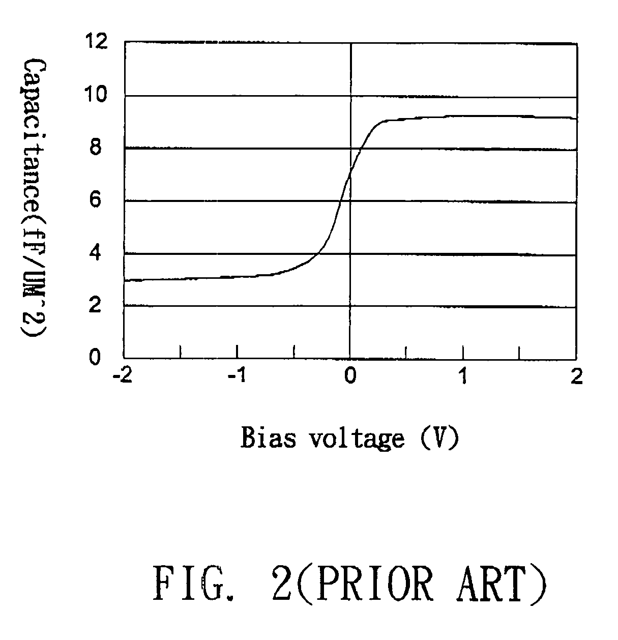
[0019]FIG. 3 is a MOS varactor structure of the invention according to the embodiment of the invention while FIG. 4 is a CV curve of the MOS varactor operated at a low frequency according to the embodiment of the invention. As shown in FIG. 3, the MOS varactor 30 of the invention, formed on a P-type substrate 31, includes a deep N well 32, a N-type low doping region 33, a N well 34, a number of first N-type high doping region 35, and a number of second N-...


PUM


Abstract

A metal oxide semiconductor (MOS) varactor includes a first terminal and a second terminal, and the MOS varactor comprises a substrate; a deep well, formed on the substrate; and a first MOS device, formed on the deep well; wherein a gate of the first MOS device is coupled to the first terminal, and a source and a drain of the first MOS device are coupled to the second terminal.

Description

[0001] This application claims the benefit of Taiwan application Serial No. 093120175, filed Jul. 6, 2004, the subject matter of which is incorporated herein by reference. BACKGROUND OF THE INVENTION [0002] 1. Field of the Invention [0003] The invention relates in general to a varactor, and more particularly to a metal oxide semiconductor (MOS) varactor. [0004] 2. Description of the Related Art [0005] The MOS varactor, an essential device in the RF IC design field, is widely applied to voltage controlled oscillator (VCO) circuit and tunable filter circuit. The tuning range is the capacitance range a varactor can provides and is defined by Cmax / Cmin. Ordinary speaking, it is preferred that the varactor has a large tuning range, and the linearity refers to whether the varactor is easily utilized. [0006]FIG. 1 is an ordinary MOS varactor structure and FIG. 2 is the capacitance / voltage (CV) curve of the MOS varactor. In the structure of the MOS varactor of FIG. 1, the tuning range is de...

Claims


Application Information

Patent Timeline
IPC IPC(8): H01L29/76H01L21/336
CPCH01L29/94H01L29/93
Inventor JEAN, YUH-SHENGYEH, TA-HSUN
Owner REALTEK SEMICON CORP
Why Eureka
Try Eureka