Plasma display panel

a technology of display panel and plasma, which is applied in the direction of discharge tube/lamp details, discharge tube luminescnet screens, gas-filled discharge tubes, etc., can solve the problems of non-uniform and faulty discharge, and achieve the effect of preventing faulty discharge, improving color purity, and less deterioration of fluorescent materials

Inactive Publication Date: 2006-01-12
SAMSUNG SDI CO LTD
View PDF14 Cites 2 Cited by
  • Summary
  • Abstract
  • Description
  • Claims
  • Application Information

AI Technical Summary

Benefits of technology

[0009] It is also an object of the present invention to provide a design for a PDP that compensates for the varying surface potential of the differently colored fluorescent materials.
[0010] It is still an object of the present invention to produce a design for a PDP that allows for the application of uniform address voltages for the differently colored subpixels.
[0011] It is still an object of the present invention to provide a design for a PDP that is capable of preventing faulty discharge and non-uniform discharge by accumulating the same amount of wall charges during the address discharge for each of the red, blue and green subpixels.
[0012] It is further an object of the present invention to provide a design for a PDP that has improved color purity and less deterioration of the fluorescent material.

Problems solved by technology

This variation in the amount of accumulated wall charges during the address discharge results in a faulty and non-uniform sustain discharge.

Method used


Image

  • Plasma display panel
  • Plasma display panel
  • Plasma display panel

Examples


Embodiment Construction

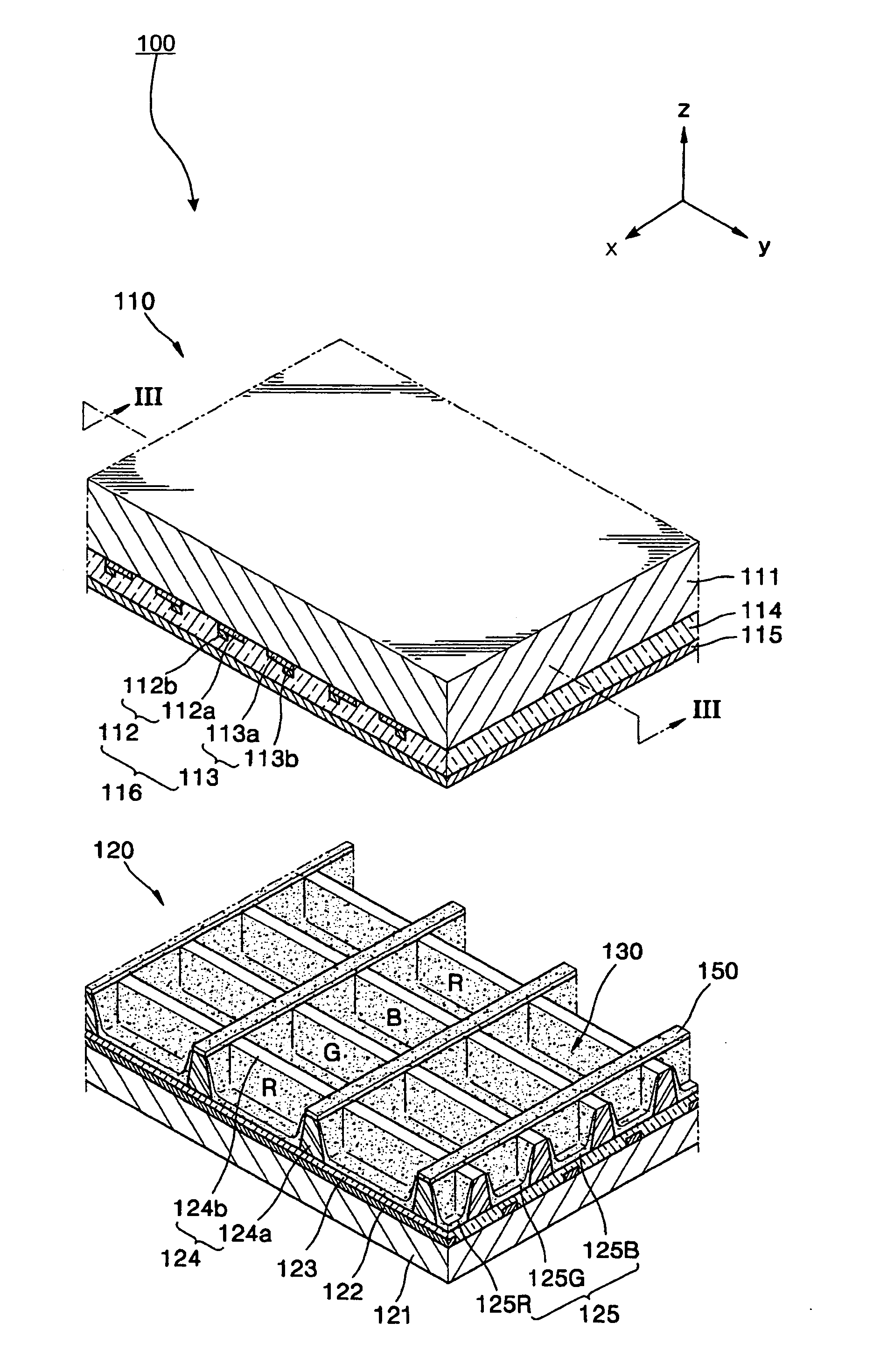
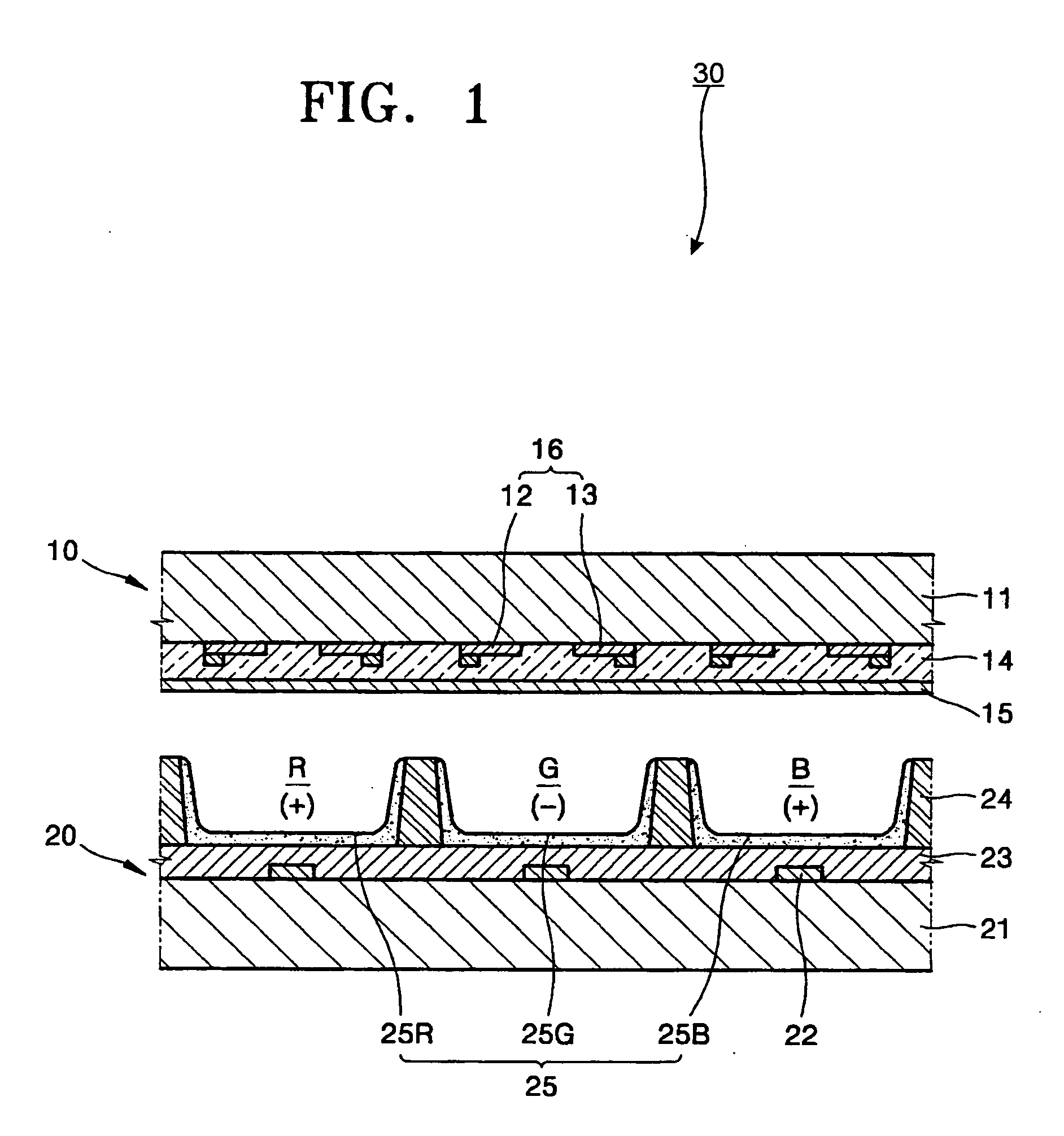
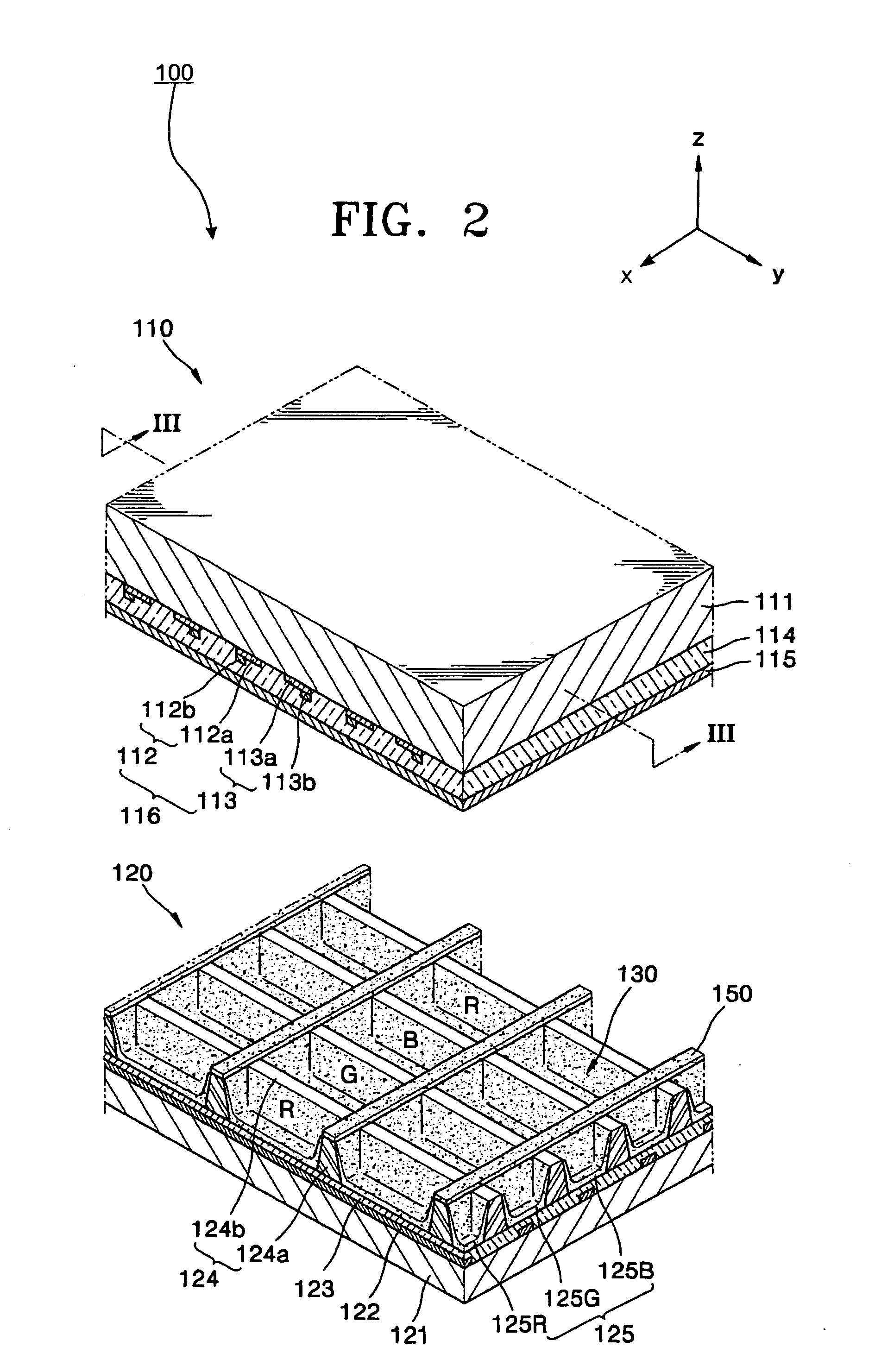
[0024] Turning now to the figures, FIG. 1 is a cross sectional view illustrating a three-electrode surface discharge type plasma display panel (PDP) 30. The PDP 30 includes an upper panel 10 and a lower panel 20 opposite to the upper panel 10. In FIG. 1, the upper panel 10 is rotated by 90 degrees with respect to the lower panel 20 for the convenience of viewing and explanation.

[0025] The upper panel 10 includes an upper substrate 11, a plurality of discharge sustain electrode pairs 16 located on a bottom surface of the upper substrate 11, an upper dielectric layer 14 covering the discharge sustain electrode pairs 16 formed on the upper substrate 11, and a protective layer 15 for covering the upper dielectric layer 14. One electrode of the discharge sustain electrode pair 16 is referred to as a sustain electrode 12 and the other is referred to as a scan electrode 13.

[0026] The lower panel 20 includes a lower substrate 21, address electrodes 22 located on the lower substrate 21 and...


PUM


Abstract

A plasma display panel capable of preventing faulty discharge and non-uniform discharge by applying a uniform address voltage to all subpixels. This is done by neutralizing the negative surface potential of a zinc silicate green fluorescent material using YBO3:Tb as a positive surface potential material on the partition walls between the electrodes. Also, the thickness of this YBO3:Tb material and a lateral spacing between a scan electrode and the positive surface potential material are carefully selected to arrive at a design resulting in no faulty pixels. Grooves can also be formed in the tops of the partition walls so that the positive surface potential material filled therein does not mix with the neighboring flourescent material.

Description

CLAIM OF PRIORITY [0001] This application makes reference to, incorporates the same herein, and claims all benefits accruing under 35 U.S.C. §119 from an application for PLASMA DISPLAY PANEL earlier filed in the Korean Intellectual Property Office on 7 Jul. 2004 and there duly assigned Serial No. 10-2004-0052606. BACKGROUND OF THE INVENTION [0002] 1. Field of the Invention [0003] The present invention pertains to a plasma display panel (PDP) having an enhanced structure capable of preventing faulty discharge and non-uniform discharge by allowing for the application of uniform address voltages to be applied to all subpixels. [0004] 2. Description of Related Art [0005] Recently, PDPs are becoming increasingly popular as next generation large flat panel displays because of the PDP's large screen size, high image quality, thin thickness, light weight, and wide viewing angle. Even more so, the large sized PDP can be more easily manufactured by a more simpler methods than other display ap...

Claims


Application Information

Patent Timeline
Patent Type & Authority Applications(United States)
IPC IPC(8): H01J17/49
CPCH01J11/12H01J2211/42H01J11/36H01J11/42
Inventor KANG, TAE-KYOUNG
Owner SAMSUNG SDI CO LTD
Why Eureka
Try Eureka