
Plasma display device and method for driving the same

a display device and plasma technology, applied in the field of display devices, can solve the problems of reducing the driving efficiency of the plasma display panel, generating erroneous discharge, unstable address discharge in the address period, etc., and achieve the effects of reducing the noise of waveforms being applied, enhancing the operational efficiency of the panel, and reducing the noise of address discharg

Inactive Publication Date: 2009-11-17
LG ELECTRONICS INC
View PDF43 Cites 2 Cited by
  • Summary
  • Abstract
  • Description
  • Claims
  • Application Information

AI Technical Summary

Benefits of technology

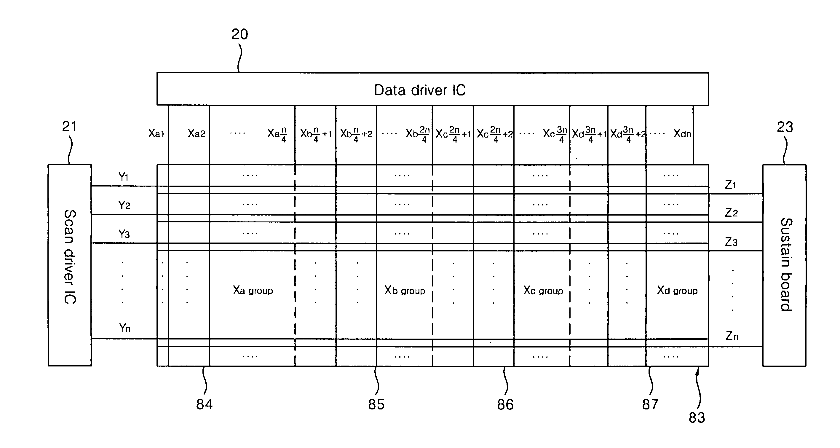
The present invention relates to a driving method for a plasma display device that reduces noise and prevents high-temperature and low-temperature erroneous discharge. The method includes steps of grounding the sustain electrode during a reset period, applying a scan signal to the scan electrode in an address period, and applying data signals to address electrode groups at different timings from the scan signal. The method can also include a pre-reset period for accumulating wall charges within a discharge cell and a negative waveform applied to the scan electrode before the reset period. The invention can improve operational efficiency of the plasma display device and enhance the stability of waveforms being applied to the scan electrode.

Problems solved by technology

These noises make the address discharge occurred in the address period unstable, and reduces the driving efficiency of the plasma display panel.
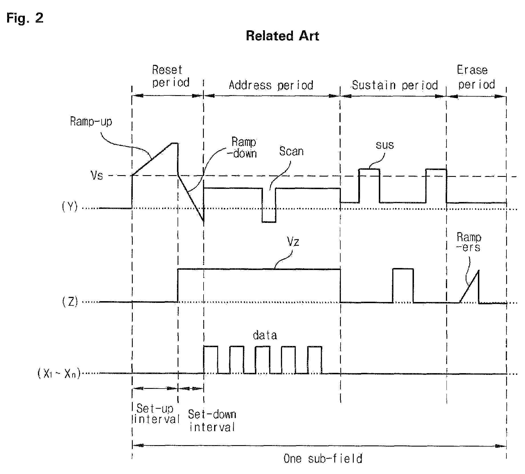
In general, the above driving waveform often generates erroneous discharge when the temperature of the panel is high or low.
In result, the absolute amount of wall charges participating in a discharge is reduced, and erroneous discharge occurs.
For example, if the recoupling rate between the space charges 701 and the wall charges 700 is increased in the address period, the amount of wall charges 700 participating in the address discharge is reduced, resulting in an unstable address discharge.
In consequence, a next sustain discharge may not be generated at all (i.e., the high-temperature erroneous discharge).
Thus, the absolute amount of seed electrons that collide with neutrons for producing other electrons is decreased, resulting in erroneous discharge.
Accordingly, the plasma discharge mechanism cannot be operated smoothly.
That is, the plasma discharge mechanism slows down and the erroneous discharge occurs.
Hence, a discharge cell that needs to be turned on in the sustain period is often turned off (i.e., the low-temperature erroneous discharge).

Method used


Image

  • Plasma display device and method for driving the same
  • Plasma display device and method for driving the same
  • Plasma display device and method for driving the same

Examples


Embodiment Construction

[0079]FIG. 7 is an illustration of a plasma display panel structure. The plasma display panel includes a front substrate 100 where a plurality of sustain electrode pairs, each pair including a scan electrode 102 and a sustain electrode 101 formed on a front glass 100 on which an image is displayed. A plurality of address electrodes 112 are arranged to intersect with the sustain electrode pairs is attached in parallel to a rear glass substrate 110, which is a predetermined distance apart from the front substrate 100.

[0080]A scan electrode 102 and a sustain electrode 101 form a pair of electrodes for generating discharge in one discharge cell and maintaining luminescence of the cell. As shown in FIG. 7, the scan electrode 102 and the sustain electrode 101 include a transparent electrode (a) made of (Indium-Tin-Oxide) ITO and a bus electrode (b) made of metallic materials. The scan electrode 102 and the sustain electrode 101 limits discharge current, and are covered by at least one upp...


PUM


Abstract

In a plasma display device, the application of at least one address signal to a cell receiving a scan signal is offset from the application of the scan signal. Such offset improves picture quality and / or reduces noise.

Description

CROSS-REFERENCE TO RELATED APPLICATIONS[0001]This Nonprovisional application claims priority under 35 U.S.C. § 119(a) on Patent Application Nos. 10-2004-0095414 and 10-2004-0103261 and 10-2004-0103877 filed in Korea on Nov. 19, 2004 and Dec. 8, 2004 and Dec. 9, 2004 the entire contents of which are hereby incorporated by reference.BACKGROUND OF THE INVENTION[0002]1. Field of the Invention[0003]The present invention relates to a display device and more particularly, a plasma display device and a driving method thereof.[0004]2. Background of the Related Art[0005]In general, a plasma display panel is formed of unit cells, and each unit cell includes a front substrate, a rear substrate and a barrier rib or a partition formed between the substrates. Each cell is filled with an inert gas mixture containing neon (Ne), helium (He) or major discharge gases such as a mixed gas of Ne+He, and a small amount of xenon. When discharge occurs by a radio frequency voltage, the inert gas generates va...

Claims


Application Information

Patent Timeline
Patent Type & Authority Patents(United States)
IPC IPC(8): G09G3/28G09G3/288G09G3/20G09G3/291G09G3/292G09G3/293G09G3/294G09G3/296G09G3/298
CPCG09G3/2022G09G3/2927G09G3/293G09G2320/041G09G2310/066G09G2320/0238G09G2310/0218
Inventor YANG, HEECHANJUNG, YUNKWONKIM, JINYOUNG
Owner LG ELECTRONICS INC
Learn More