Semiconductor integrated circuit device and a method of manufacturing the same

Active Publication Date: 2006-01-12
RENESAS ELECTRONICS CORP
View PDF22 Cites 32 Cited by
  • Summary
  • Abstract
  • Description
  • Claims
  • Application Information

AI Technical Summary

Benefits of technology

[0040] According to the above means, the first negative voltage is applied to the first well region to thereby form the reverse-direction voltage applied state (reverse bias state) between the second gate electrode and the memory electrode near the second gate electrode, thereby making it possible to generate hot holes and hot electrons by band-to-band tunneling. The electric field for directing the first polarity charge, e.g., hot holes from the well region side to the charge storage region is formed to thereby produce an avalanche of the hot holes, so that a relatively large number of the hot holes are injecte

Problems solved by technology

A first problem resides in the fact that the drain current at the time of a reading operation in a low threshold voltage state is small.
This problem results in a large drawback in a logic-mixed flash memory module which needs

Method used


Image

  • Semiconductor integrated circuit device and a method of manufacturing the same
  • Semiconductor integrated circuit device and a method of manufacturing the same
  • Semiconductor integrated circuit device and a method of manufacturing the same

Examples


Embodiment Construction

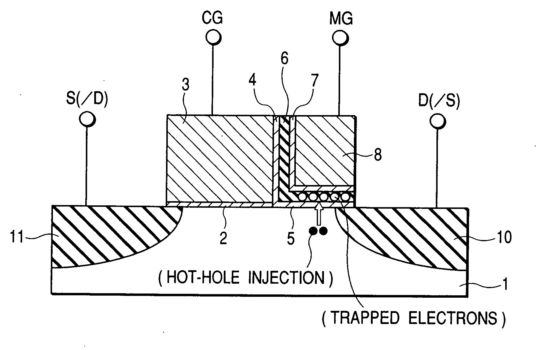
[0181] Preferred embodiments of the present invention will be described in detail with reference to the accompanying drawings. Incidentally, components having the same function in all of the drawings are respectively identified by the same reference numerals, and their repetitive description will be omitted. In the following description, a MOS (Metal Oxide Semiconductor) transistor (also simply described as “MOS”) will be used as one example of MIS transistors (or MISFET), which are generic names for insulated gate field effect transistors.

>

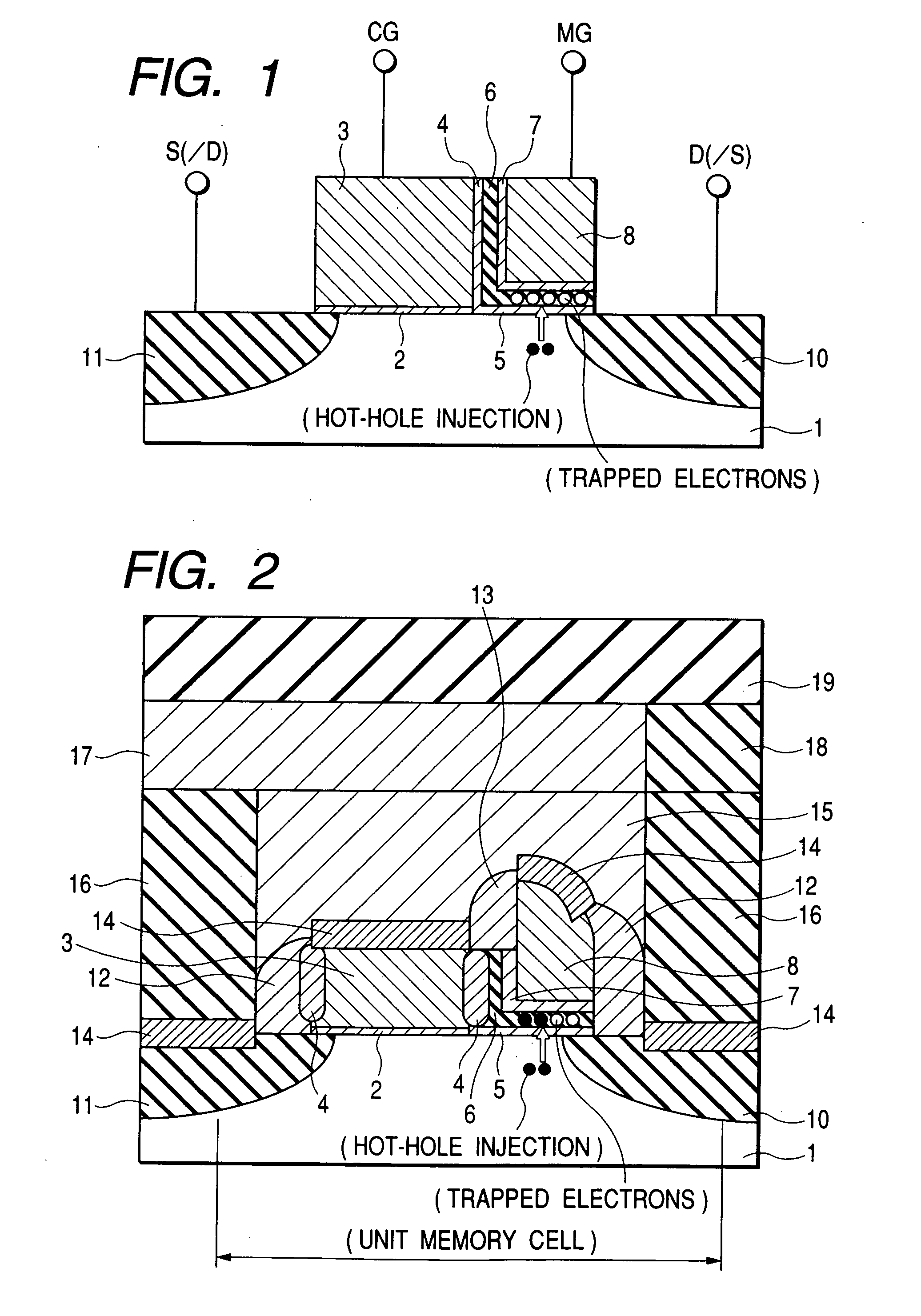
[0182] A nonvolatile memory cell transistor (also simply called a “memory cell”) applied to a semiconductor integrated circuit device according to the present invention is illustrated in FIG. 1 in the form of a vertical cross-section. A first structural viewpoint related to the memory cell transistor resides in writing and erasure operations based on electron- and hot-hole injection, and a split gate structure. Namely, the memory cell transistor...


PUM


Abstract

The memory cell transistor includes, in a first well region, a pair of memory electrodes, one of which serves as source electrode and the other serves as drain electrode and a channel region interposed between the pair of memory electrodes. There is, on a channel region, a first gate electrode disposed near its corresponding memory electrode with an insulating film interposed therebetween, and a second gate electrode disposed through insulating films and a charge storage region and electrically isolated from the first gate electrode. A first negative voltage is applied to the first well region to form a state of reverse bias greater than or equal to a junction withstand voltage between the second gate electrode and the memory electrode near the second gate electrode, thereby enabling injection of hot electrons into the charge storage region and injection of electrons from the well region to the charge storage region.

Description

[0001] This application is a Continuation of U.S. patent application Ser. No. 10 / 400,469, filed Mar. 28, 2003, the entire disclosure of which is hereby incorporated by reference.TECHNICAL FIELD [0002] The present invention relates in general to a semiconductor integrated circuit device having a nonvolatile memory cell transistor (nonvolatile memory element), and to a method of manufacture thereof; and, more particularly, the invention relates, for example, to a technology that is effective when applied to a semiconductor integrated circuit device equipped with an on-chip nonvolatile memory, using a nonconductive charge trap film in an information retention region together with a CPU (Central Processing Unit). BACKGROUND OF THE INVENTION [0003] As a memory device for storing data or program-configured data, attention has recently been focused on a flash EEPROM (hereinafter called a “flash memory”), which is defined as a nonvolatile memory device that is capable of electrically erasin...

Claims


Application Information

Patent Timeline
IPC IPC(8): H01L21/336H01L21/3205G11C16/04G11C16/10G11C16/14G11C16/26H01L21/8234H01L21/8246H01L21/8247H01L27/088H01L27/10H01L27/105H01L29/788H01L29/792
CPCB82Y10/00H01L29/792G11C16/14G11C16/26G11C16/34H01L21/28273H01L21/28282H01L27/0207H01L27/105H01L27/115H01L27/11521H01L27/11526H01L27/11546H01L27/11568H01L27/11573H01L29/42344H01L29/66825H01L29/66833G11C16/10H01L2924/0002H01L29/40114H01L29/40117H10B69/00H10B41/30H10B41/40H10B41/49H10B43/30H10B43/40H01L2924/00H01L29/42328H01L29/45H10B43/35H01L23/535H01L29/42368G11C16/0466H01L29/4975H01L29/513H01L29/518
Inventor SHUKURI, SHOJI
Owner RENESAS ELECTRONICS CORP
Why Eureka
Try Eureka