Unlock instant, AI-driven research and patent intelligence for your innovation.

Method and apparatus for classifying repetitive defects on a substrate

a technology of repetitive defects and apparatus, which is applied in the direction of material analysis, semiconductor/solid-state device testing/measurement, instruments, etc., can solve the problems of long time required for performing the conventional method and difficulty in finding the contamination sources of semiconductor device defects, etc., and achieve the effect of short tim

Inactive Publication Date: 2006-01-19
SAMSUNG ELECTRONICS CO LTD
View PDF3 Cites 10 Cited by
  • Summary
  • Abstract
  • Description
  • Claims
  • Application Information

AI Technical Summary

Benefits of technology

[0014] The present invention provides a method of classifying repetitive defects on a substrate in a relatively short time. The present invention also provides a method of classifying repetitive defects on a substrate that is capable of accurately classifying repetitive defects separately from all of the other defects on the substrate. The present invention still also provides an apparatus for performing the above-mentioned method.

Problems solved by technology

Thus, it is very difficult to find the contamination sources which provide defects in the semiconductor device, since hundreds of processes are performed in manufacturing a semiconductor device.
Thus, the time required for performing the conventional method is too long.
However, in the conventional method, since the defects are not classified according to shot region, the recognized defects are mistakenly classified as the repetitive defects, and the normal reticle is determined to be abnormal.

Method used


Image

  • Method and apparatus for classifying repetitive defects on a substrate
  • Method and apparatus for classifying repetitive defects on a substrate
  • Method and apparatus for classifying repetitive defects on a substrate

Examples


embodiment 1

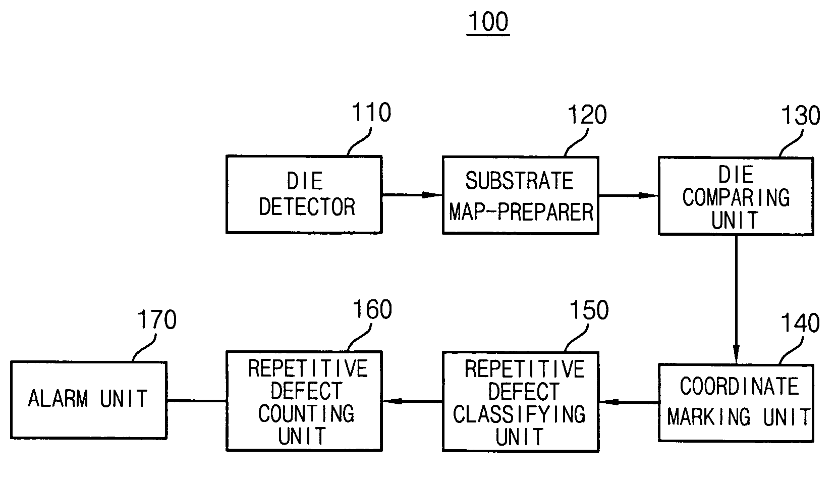
[0040] Referring to FIG. 4, an apparatus 100 for classifying repetitive defects in accordance with the present embodiment receives information from a defect-detecting unit. The defect-detecting unit includes a defect detector 110 for detecting all of the defects on a semiconductor substrate and a map preparer 120 for preparing a map of the semiconductor substrate on which positions of all of the defects detected by the defect detector 110 are marked.

[0041] Referring to FIG. 5, the map preparer 120 prepares the substrate map on which the positions of all of the defects are marked. Here, the semiconductor substrate W is divided into a plurality of dies D. The substrate map is provided to the classifying apparatus 100.

[0042] Referring now to FIG. 4, the classifying apparatus 100 includes a die-comparing unit 130 for comparing the dies D on the substrate map with a reference die, a coordinate-marking unit 140 for marking the positions of all of the defects on the reference die, and a ...

embodiment 2

[0067] Referring to FIG. 10, an apparatus 200 for classifying repetitive defects in accordance with the present embodiment includes a defect detector 210 for detecting all of the defects on a semiconductor substrate and a map preparer 220 for preparing a map of the semiconductor substrate on which positions of all of the defects detected by the defect detector 210 are marked.

[0068] Referring to FIG. 11, the map preparer 220 prepares the substrate map on which the positions of all of the defects are marked. Here, the semiconductor substrate W is divided into a plurality of process regions E. Each of the process regions includes a plurality of dies D. The substrate map is provided to the classifying apparatus 200.

[0069] Referring now to FIG. 10, the classifying apparatus 200 includes a die-comparing unit 230 for comparing the dies D on the substrate map with a reference die, a coordinate-marking unit 240 for marking the positions of all of the defects on the reference die, a process...

embodiment 3

[0094]FIG. 13 is a block diagram illustrating an apparatus for classifying repetitive defects in accordance with a third embodiment of the present invention.

[0095] Referring to FIG. 13, an apparatus 300 for classifying repetitive defects in accordance with the present embodiment includes a defect detector 310 for detecting all of the defects on a semiconductor substrate and a map preparer 320 for preparing a map of the semiconductor substrate on which positions of all of the defects detected by the defect detector 310 are marked.

[0096] The classifying apparatus 300 includes a process region-comparing unit 330 for comparing the process regions on the substrate map with a reference process region, a coordinate-marking unit 340 for marking the positions of all of the defects on the reference process region, and a repetitive defect-classifying unit 350 for classifying repetitive defects separately from all of the other defects.

[0097] Additionally, the classifying apparatus 300 may fu...


PUM

PropertyMeasurementUnit
timeaaaaaaaaaa
shapeaaaaaaaaaa
specific wavelengthaaaaaaaaaa

Abstract

A method and apparatus of classifying repetitive defects on a substrate is provided. Defects of dies on the substrate are sequentially compared with a predetermined reference die. Sets of coordinates are marked on the reference die which are corresponding to the position of the defects on the dies on the substrate. Then, repetitive defects are classified which are repeatedly marked in a specified region on the reference die.

Description

CROSS REFERENCE TO RELATED APPLICATION [0001] This application claims priority under 35 USC § 119 to Korean Patent Application No. 2004-54346, filed on Jul. 13, 2004, the contents of which are herein incorporated by reference in its entirety for all purposes. BACKGROUND OF THE INVENTION [0002] 1. Field of the Invention [0003] The present invention relates to a method and an apparatus for classifying repetitive defects on a substrate. More particularly, the present invention relates to an apparatus and method for classifying defects on dies of a substrate into repetitive defects and non-repetitive defects, and an apparatus for performing the method. [0004] 2. Description of the Related Art [0005] Generally, a semiconductor device is manufactured under surroundings that include various contamination sources such as particles in air, contaminants generated from process equipment, reactants and / or products, etc. Thus, it is very difficult to find the contamination sources which provide ...

Claims


Application Information

Patent Timeline
Patent Type & Authority Applications(United States)
IPC IPC(8): G01N21/88
CPCG01N21/95607G01N21/9501H01L22/00
Inventor LIM, YOUNG-KYULEE, BYUNG-AMAHN, BYUNG-SEOLCHO, JAE-SUNLEE, CHANG-HOONLEE, JUNG-LANLEE, SUNG-MAN
Owner SAMSUNG ELECTRONICS CO LTD
Features
  • R&D
  • Intellectual Property
  • Life Sciences
  • Materials
  • Tech Scout
  • Unparalleled Data Quality
  • Higher Quality Content
  • 60% Fewer Hallucinations
Learn More