

Manufacturing method for semiconductor devices, arrangement determination method and apparatus for semiconductor device formation regions, and program for determining arrangement of semiconductor device formation regions
- Summary
- Abstract
- Description
- Claims
- Application Information
AI Technical Summary
Benefits of technology
Problems solved by technology
Method used
Image

Examples
Embodiment Construction
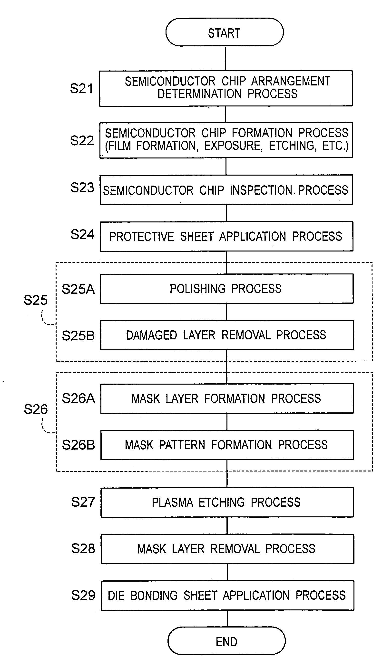
[0089] Before the description of the present invention proceeds, it is to be noted that like parts are designated by like reference numerals throughout the accompanying drawings.
[0090] The embodiment of the present invention will be hereinbelow described in detail with reference to the drawings.
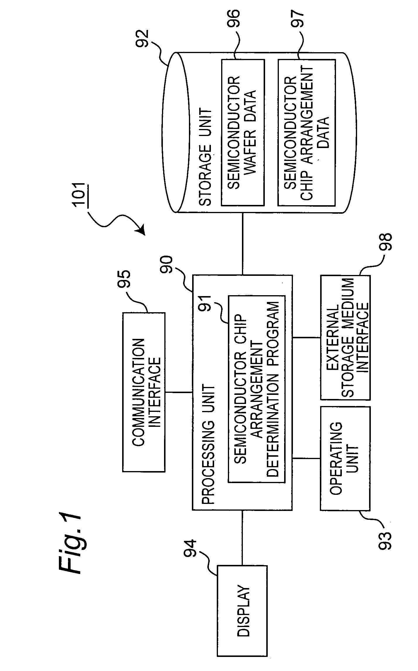
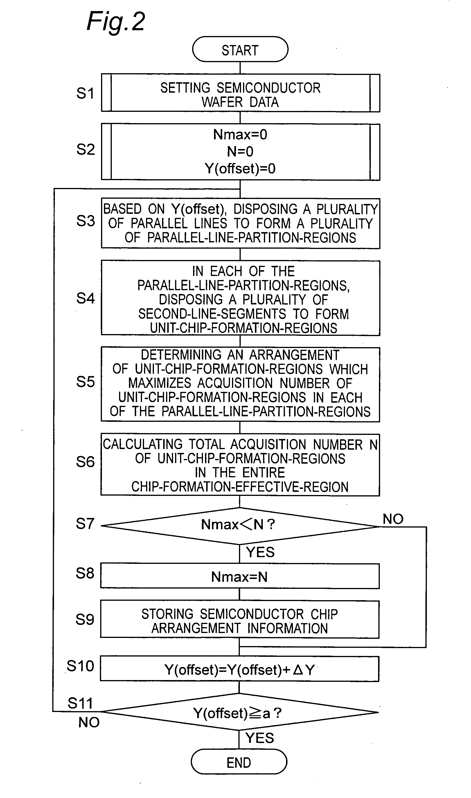
[0091]FIG. 1 is a block diagram showing an outlined configuration of a semiconductor chip arrangement determination apparatus 101 exemplifying an arrangement determination apparatus for semiconductor device formation regions according to an embodiment of the present invention. With reference to FIG. 1, description will be hereinbelow given of the outlined configuration of the semiconductor chip arrangement determination apparatus 101.
[0092] As shown in FIG. 1, the semiconductor chip arrangement determination apparatus 101 has a processing unit 90 for executing a semiconductor chip (semiconductor device) arrangement determination program 91 to perform arrangement determination processing fo...
PUM
 Abstract
Description
Claims
Application Information