Dual gas faceplate for a showerhead in a semiconductor wafer processing system

a technology of semiconductor wafers and showerheads, applied in the direction of electric discharge tubes, coatings, chemical vapor deposition coatings, etc., can solve the problems of o-ring material breakdown, contamination of the chamber and even the wafer surface, and achieve uniform gas distribution

Inactive Publication Date: 2006-02-02
APPLIED MATERIALS INC
View PDF97 Cites 526 Cited by
  • Summary
  • Abstract
  • Description
  • Claims
  • Application Information

AI Technical Summary

Benefits of technology

This patent describes an apparatus used in semiconductor manufacturing processes where two layers are used to distribute gas during chemical reactions. These layers have many small openings called gas holes which allow the gas to flow uniformly throughout the reaction area. By feeding different types of gas through these holes at specific locations, researchers can better control the growth of materials on the substrate being processed. This design ensures a purer and more accurate delivery of the desired gas mixture, resulting in higher quality films and devices made from those processes.

Problems solved by technology

The technical problem addressed in this patent is how to deliver multiple gases to a semiconductor wafer processing system without allowing them to mix before entering the process region, while also eliminating the use of elastic or soft O-rings to seal the gases within the showerhead. There is also a need for a double gas facplate made from a solid Nickel material.

Method used


Image

  • Dual gas faceplate for a showerhead in a semiconductor wafer processing system
  • Dual gas faceplate for a showerhead in a semiconductor wafer processing system
  • Dual gas faceplate for a showerhead in a semiconductor wafer processing system

Examples


Embodiment Construction

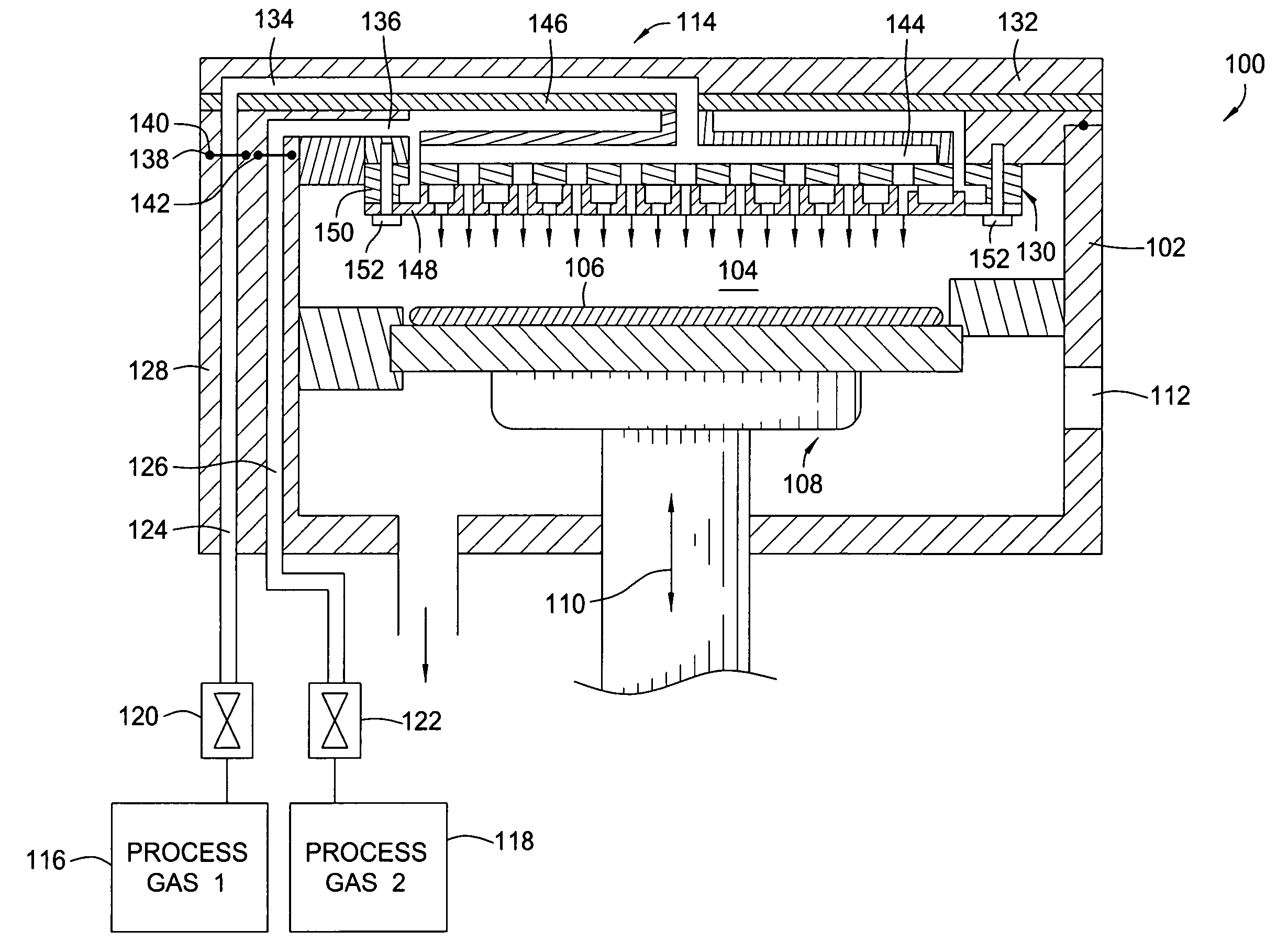
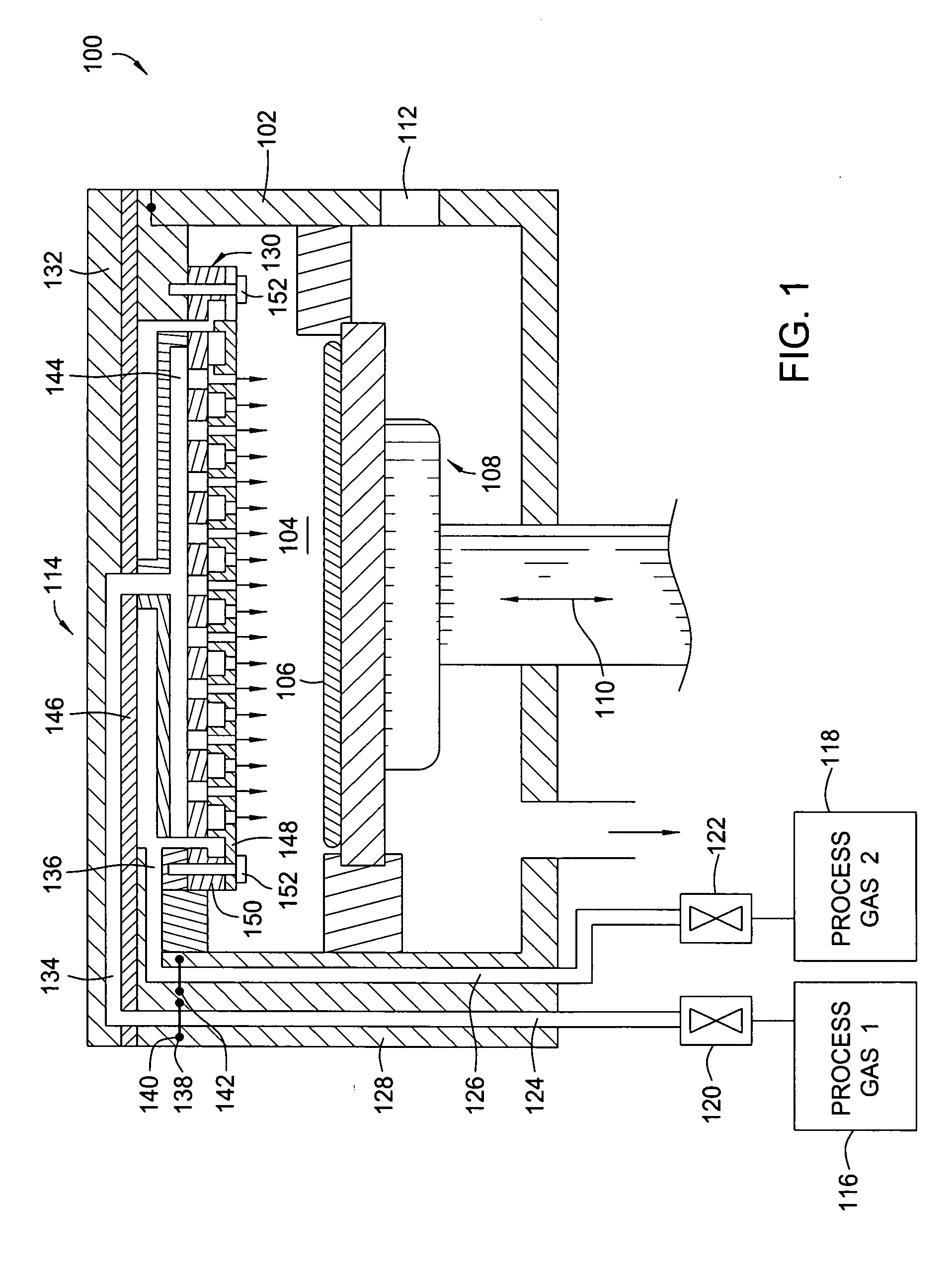
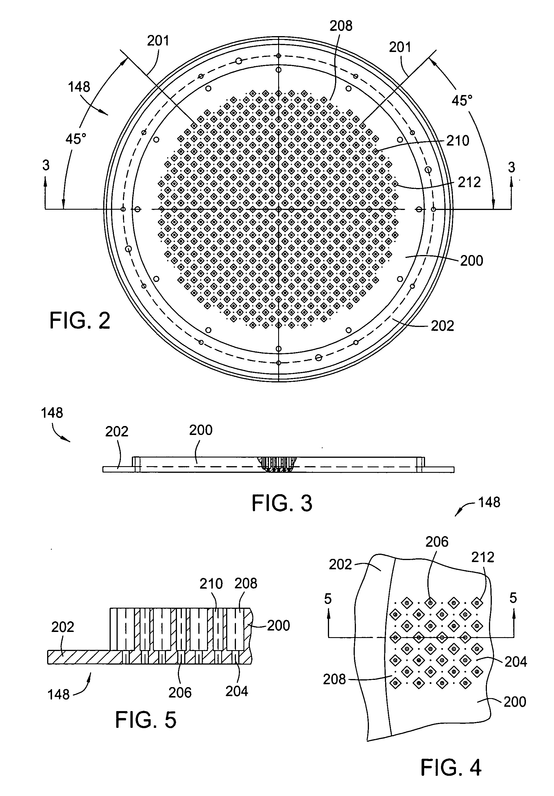
[0035]FIG. 1 depicts a cross-sectional schematic view of a semiconductor wafer processing reaction chamber, for example, a chemical vapor deposition reactor 100. The reactor 100 contains an enclosure 102 (also generally referred to as a chamber) defining a process region 104. A substrate 106, such as a semiconductor wafer, is maintained proximate the process region 104 upon a pedestal 108. The pedestal 108 moves vertically (as indicated by arrow 110) within the enclosure 102 to lower the pedestal to a position that allows the substrate 106 to be removed through a slit valve 112. While in the lowered position, a new substrate 106 positioned upon the pedestal 108. Thereafter, the pedestal 108 is raised into a process position, as shown, which places the wafer 106 proximate the process region 104. Process gases are supplied through the showerhead 114. In the preferred embodiment of the invention a plurality of gases are used to process the wafer, illustratively, two gases are used, pro...


PUM

PropertyMeasurementUnit
Timeaaaaaaaaaa

Abstract

A faceplate for a showerhead of a semiconductor wafer processing system is provided. The faceplate has a plurality of gas passageways to provide a plurality of gases to the process region without commingling those gases before they reach the processing region within a reaction chamber. The showerhead includes a faceplate and a gas distribution manifold assembly. The faceplate defines a plurality of first gas holes that carry a first gas from the manifold assembly through the faceplate to the process region, and a plurality of channels that couple a plurality of second gas holes to a radial plenum that receives the second gas from the manifold assembly. The faceplate and the manifold assembly are each fabricated from a substantially solid nickel material.

Description


Claims


Application Information

Patent Timeline
Owner APPLIED MATERIALS INC
Why Eureka
Try Eureka