Dry etching method using polymer mask selectively formed by CO gas

a technology of selective etching and polymer mask, which is applied in the direction of semiconductor devices, electrical equipment, basic electric elements, etc., can solve the problems of difficult to form fine patterns using a conventional photolithography process, difficult to form photoresist patterns having a good profile, and complicated manufacturing processes of semiconductor devices. achieve excellent etching profile and high resolution

Inactive Publication Date: 2006-02-02
SAMSUNG ELECTRONICS CO LTD
View PDF12 Cites 6 Cited by
  • Summary
  • Abstract
  • Description
  • Claims
  • Application Information

AI Technical Summary

Benefits of technology

[0008] Exemplary embodiments of the present invention include dry etching methods that use an etch mask selectively formed on a thin photoresist pattern so that high resolution and an excellent etching profile can be achieved.
[0013] The step of supplying the carbon monoxide gas to deposit polymer and the step of etching the etching target layer can be repeatedly performed to etch the etching target layer to a predetermined depth. The etching target layer can be formed of a material capable of preventing a polymer reaction between the etching target layer and the carbon monoxide gas.

Problems solved by technology

Manufacturing processes of semiconductor devices become more complicated as semiconductor integrated circuits (ICs) become more highly integrated.
However, it is difficult to form fine patterns using a conventional photolithography process because a line width of patterns is smaller than resolution limitation.
It is also difficult to form a photoresist pattern having a good profile in the conventional photolithography process.
However, due to a poor etching resistance, thin photoresist patterns cannot properly function as an etch mask for an underlying target layer such that a reduction in an etching depth of the target layer may occur.
Thus, as shown in FIG. 1C, the residual photoresist pattern 12′ cannot properly function as an etch mask, thereby resulting in the poor profile of the etch layer 11.

Method used


Image

  • Dry etching method using polymer mask selectively formed by CO gas
  • Dry etching method using polymer mask selectively formed by CO gas
  • Dry etching method using polymer mask selectively formed by CO gas

Examples


Embodiment Construction

[0024] Exemplary embodiments of the present invention will now be described more fully hereinafter below with reference to the accompanying drawings. This invention may, however, be embodied in different forms and should not be construed as limited to the exemplary embodiments set forth herein. Rather, these exemplary embodiments are provided so that this disclosure will be through and complete, and will fully convey the scope of the invention to those skilled in the art.

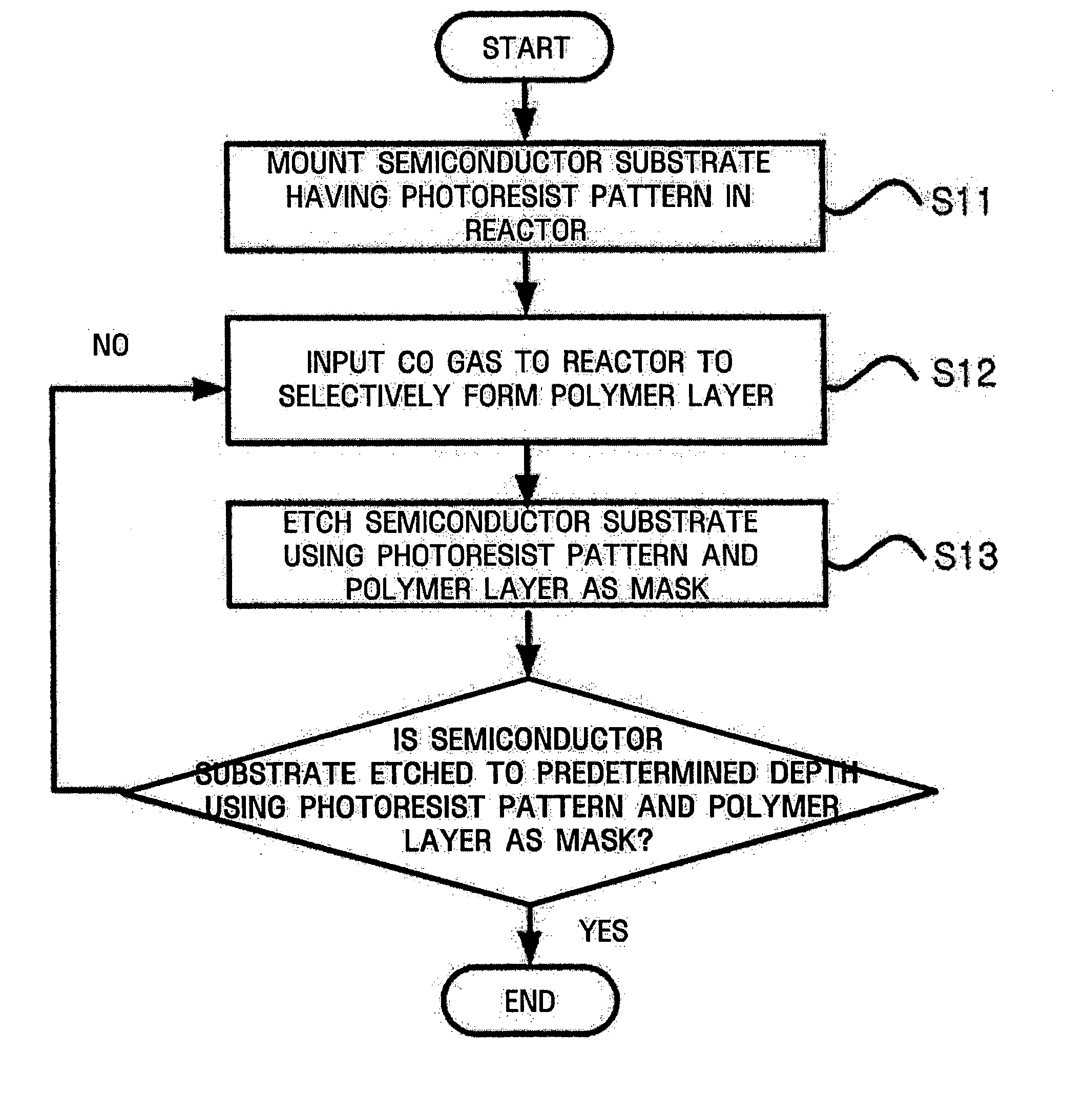
[0025] A dry etching method according to an exemplary embodiment of the present invention is described with reference to FIG. 2 through FIG. 7. Referring to FIG. 2, a semiconductor substrate having a photoresist pattern formed on an etching target layer is placed in a reactor (S11). Referring to FIG. 3, an etching target layer 31 is formed on a semiconductor substrate 30 by chemical vapor deposition (CVD). The etching target layer 31 may be formed of a material that can prevent a polymer reaction between the etchin...


PUM


Abstract

A dry etching method comprises placing a semiconductor substrate in a reactor, the semiconductor substrate comprising a photoresist pattern formed on an etching target layer, supplying carbon monoxide gas into the reactor to selectively deposit polymer on the photoresist pattern to form a polymer layer, and etching the etching target layer using the photoresist pattern and the polymer layer as an etch mask.

Description

CROSS-REFERENCE TO RELATED APPLICATION [0001] This application claims priority to Korean Patent Application No. 10-2004-0060275 filed on Jul. 30, 2004, the disclosure of which is incorporated herein by reference in its entirety. TECHNICAL FIELD [0002] The present disclosure relates to a method of manufacturing a semiconductor device, and more particularly to a dry etching method using a polymer mask selectively formed on a photoresist pattern by carbon monoxide (CO) gas. BACKGROUND [0003] Manufacturing processes of semiconductor devices become more complicated as semiconductor integrated circuits (ICs) become more highly integrated. Thus, semiconductor devices capable of forming ultra-fine patterns are needed by developing a new photoresist material suitable for forming the ultra-fine patterns. However, it is difficult to form fine patterns using a conventional photolithography process because a line width of patterns is smaller than resolution limitation. It is also difficult to fo...

Claims


Application Information

Patent Timeline
Patent Type & Authority Applications(United States)
IPC IPC(8): H01L21/461H01L21/302
CPCH01L21/0273H01L21/3081H01L21/3085H01L2221/1057H01L21/32139H01L21/76802H01L21/31144H01L21/306
Inventor PARK, WAN-JAECHANG, HO-SENOH, YOUNG-MOOK
Owner SAMSUNG ELECTRONICS CO LTD
Why Eureka
Try Eureka