TEM MEMS device holder and method of fabrication

Inactive Publication Date: 2006-02-02
THE BOARD OF TRUSTEES OF THE UNIV OF ILLINOIS +2
View PDF7 Cites 60 Cited by
  • Summary
  • Abstract
  • Description
  • Claims
  • Application Information

AI Technical Summary

Problems solved by technology

A TEM is a relatively complex instrument, and requires precise positioning of a sample.
This places limitations on the types of samples and sample holders that may be examined

Method used


Image

  • TEM MEMS device holder and method of fabrication
  • TEM MEMS device holder and method of fabrication
  • TEM MEMS device holder and method of fabrication

Examples


first embodiment

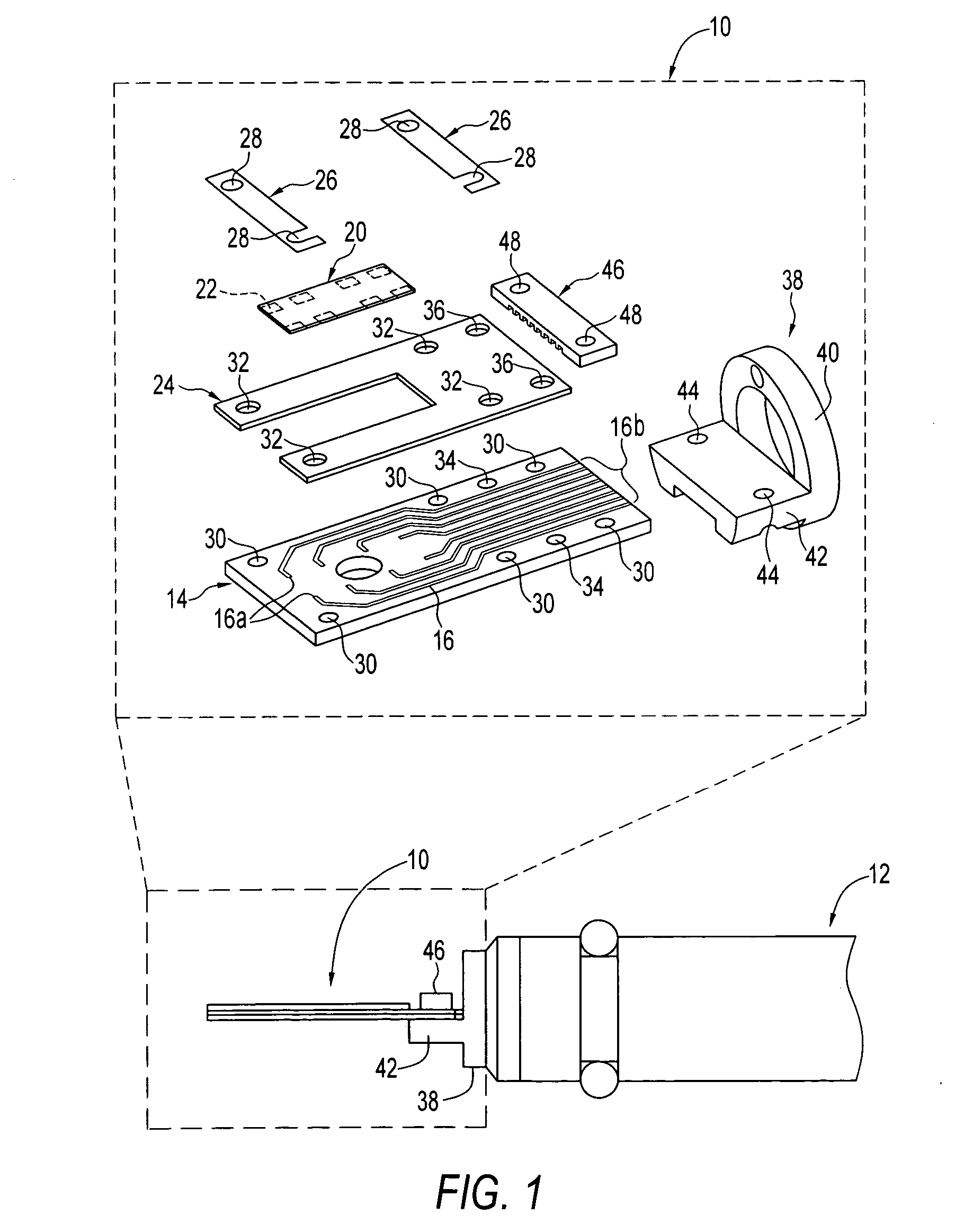
[0008]FIG. 1 is an exploded perspective view of a device holder according to the invention;

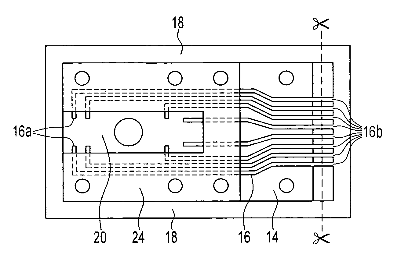
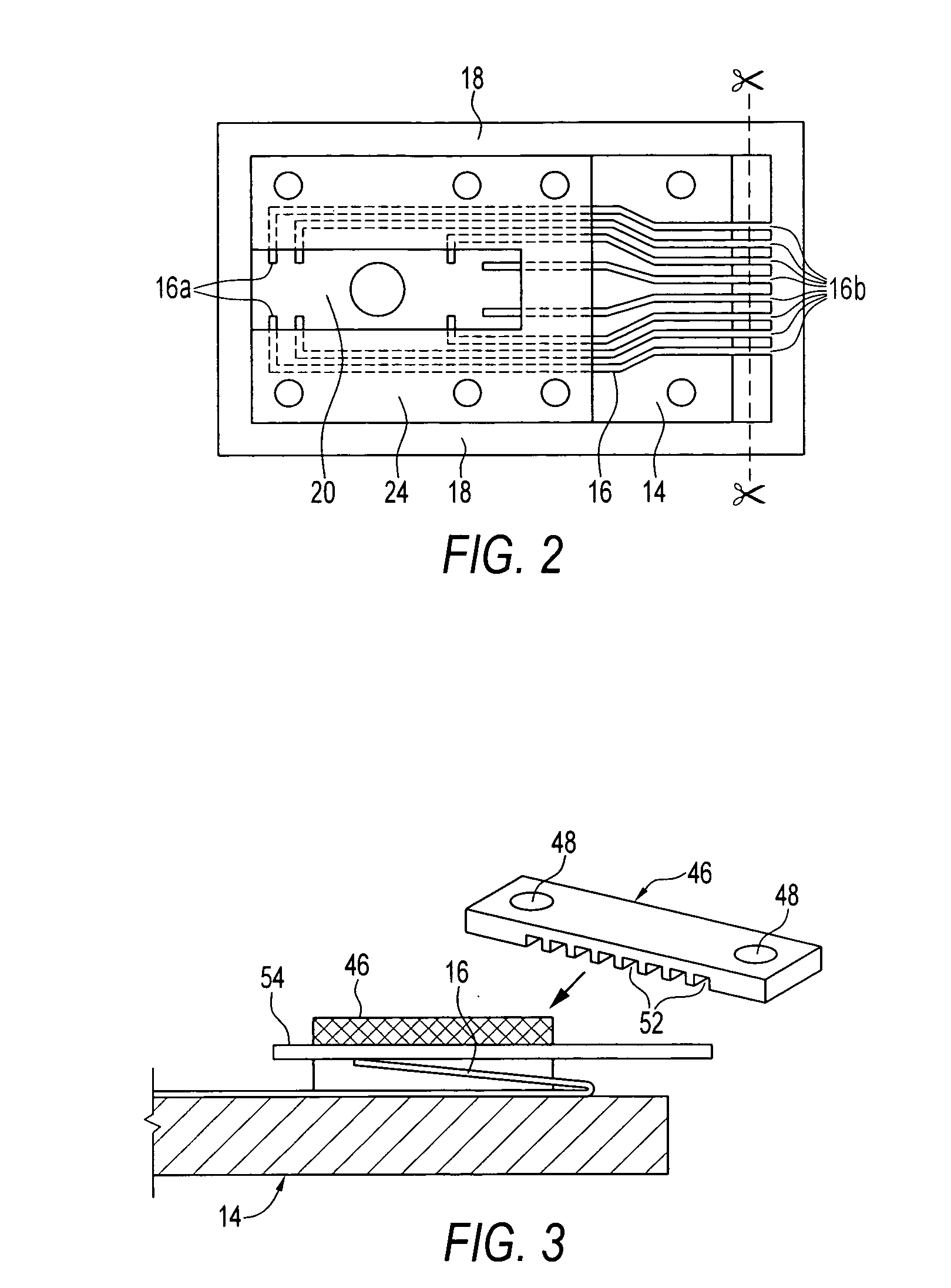
[0009]FIG. 2 is a top elevational view of the device holder illustrated in FIG. 1;

[0010]FIG. 3 is a side elevational view of the device holder illustrated in FIG. 1 in contact with a TEM wire;

[0011]FIG. 4 is a top elevational view of an exemplary MEMS devices that can be used with the device holder of FIG. 1;

second embodiment

[0012]FIG. 5A is a top elevational view of a device holder according to the invention;

[0013]FIG. 5B is a side elevational view of the device holder illustrated in FIG. 5A;

[0014]FIG. 6 is a top elevational view of an electrical contact template with the device holder of FIG. 5A;

[0015]FIG. 7 is a top elevational view of the electrical contact template of FIG. 6;

[0016]FIG. 8 is a graph illustrating heat capacity measurements on a Bi nanoparticle sample using a device holder according to embodiments of the invention, with an inset of bright field TEM micrograph of the particles;

[0017]FIG. 9 is a graph illustrating use of a nanocalorimeter as a microheater according to embodiments of the invention; and

third embodiment

[0018]FIG. 10 is an exploded perspective view of the device holder of the invention.

DETAILED DESCRIPTION OF THE PREFERRED EMBODIMENTS

[0019] There has been a growing tendency to use the transmission electron microscope (TEM) as a dynamic research tool to study atomic-scale mechanisms of complex materials processes. However, broad use of the TEM for this purpose has been limited by the relatively small space available in the objective lens pole piece of the TEM for incorporating a device holder.

[0020] In various embodiments of the invention, microelectromechanical systems (MEMS) devices are configured to be held in the sample position required by a TEM, and the invention includes a device holder that positions a MEMS device in the sample position of the TEM. MEMS devices, include, for example, miniaturized sensors and actuators for designed critical applications, and also may include fluid communication channels and other operations that can deliver samples of interest to an observa...


PUM


Abstract

A device and method for fabricating a device holder for use with a standard holder body of a transmission electron microscope for use with in situ microscopy of both static and dynamic mechanisms. One or more electrical contact fingers is disposed between a baseplate and a frame, with a MEMS device making contact with the electrical contact fingers. A connector is provided to matingly engage the transmission electron microscope and the device holder to couple the device holder to the transmission electron microscope. Once clamped between the baseplate and frame, the electrical contact fingers may be separated from the template.

Description

PRIORITY CLAIM [0001] This application claims the benefit of U.S. Provisional Application Ser. No. 60 / 591,716, filed Jul. 28, 2004, under 35 U.S.C. § 19.STATEMENT OF GOVERNMENTAL INTEREST [0002] This invention was made with Government support under Contract Number DEFG02-91-ER45439 and DEAC03-76SF00098 awarded by the Department of Energy (DOE). The Government has certain rights in the invention.FIELD OF THE INVENTION [0003] A field of the invention is transmission electron microscopy (TEM). BACKGROUND OF THE INVENTION [0004] Transmission electron microscopy (TEM) is an important technique to achieve microanalysis down to atomic level. Commonly used TEM techniques are bright field (BF) image, dark field (DF) image, high-resolution (HRTEM) image, and selected area diffraction (SAD). An analytical TEM is capable of additional complex microanalyses, e.g., convergent beam electron diffraction (CBED), z-contrast imaging (also called STEM), electron energy loss spectrum (EELS), energy disp...

Claims


Application Information

Patent Timeline
IPC IPC(8): H01R13/62
CPCH01J37/20H01R13/2442H01J2237/26H01J2237/2002
Inventor ZHANG, MINGPETROV, IVANWEN, JIANGUOSTACH, ERIC A.ALLEN, LESLIE H.ROBERTSON, IANOLSON, ERIC A.
Owner THE BOARD OF TRUSTEES OF THE UNIV OF ILLINOIS
Why Eureka
Try Eureka