Method for doping semiconductor layer, method for manufacturing thin film semiconductor device, and thin film semiconductor device

a semiconductor layer and manufacturing method technology, applied in semiconductor devices, instruments, electrical devices, etc., can solve the problems of high leakage current, low display quality, and high current off, and achieve good reproducibility and low concentration impurity diffusion

Inactive Publication Date: 2006-02-09
MACHIDA AKIO +2
View PDF12 Cites 15 Cited by
  • Summary
  • Abstract
  • Description
  • Claims
  • Application Information

AI Technical Summary

Benefits of technology

[0021] Other and further objects, features and advantages of the invention will appear more fully from the following description.

Problems solved by technology

On the other hand, when using poly-Si TFT in switching elements for pixel selection of the liquid crystal display or the like, the off current is high and display quality is low, which is a problem.
However, with the poly-Si TFT, a problem arises that a high leakage current occurs since current flows through the grain boundary of crystalline particles composing the semiconductor film or through the defects of the particles themselves.
However, in the poly-Si TFT using for the active matrix liquid crystal displays, for example, the leakage current poses a big problem since it is used under the reverse bias of about 10 V or more.
Such a problem is especially important for the thin film transistor for pixel selection of the liquid crystal displays in which the poly-Si is used.
When forming the thin film transistor having the LDD structure by such a method, there is a problem of the difference or the variation in lengths of the LDDs on both sides of the channel region (thicknesses of the LDD regions between the channel regions and contact regions) due to deviation of the mask during patterning of the gate electrode, and the like.
This causes other problems that the characteristics of the thin film transistor vary and the productivity of the thin film transistor decrease.
For this reason, the resistance of the LDD regions becomes high, and the carrier mobility decreases, which is a problem.
That is, it is difficult to use a glass substrate with a comparatively low melting point in the manufacturing process.
Although the ion doping and the plasma doping are advantageous to the formation of the larger area type, these processes pose problems that the film can contain hydrogen in large quantities which can blow off and break the film at the time of crystallization by the excimer laser (ELA: Excimer Laser Anneal), and that it is difficult to perform the lower temperature process using the plastic substrate or the like at the required temperature for dehydrogenation (400° C.).
Moreover, there is also a problem that these methods are not suitable for the self-alignment type process in principle.
However, in principle, it is difficult to precisely control the dose of 1×10¹⁴ / cm2 or less of the impurities.
Furthermore, since the adsorption of the impurity ion of the atomic layer occurs for an extremely short time in the conventional methods, the control at the low dose is difficult.
As seen in FIG. 13, even when the partial pressure of phosphine is changed, the sheet resistance ρs changes little and it reveals that controlling the partial pressure cannot control the concentration of impurities in an impurity diffusion region.
However, it is difficult to apply such a method to the plastic substrate considering the thermal conductivity and electrical conductivity of the plastic substrate.
Moreover, there are other problems that the impurities cannot be implanted into the semiconductor thin film with the large area all at once, and that the throughput gets worse in the manufacturing the large-sized liquid crystal displays.

Method used


Image

  • Method for doping semiconductor layer, method for manufacturing thin film semiconductor device, and thin film semiconductor device
  • Method for doping semiconductor layer, method for manufacturing thin film semiconductor device, and thin film semiconductor device
  • Method for doping semiconductor layer, method for manufacturing thin film semiconductor device, and thin film semiconductor device

Examples


Embodiment Construction

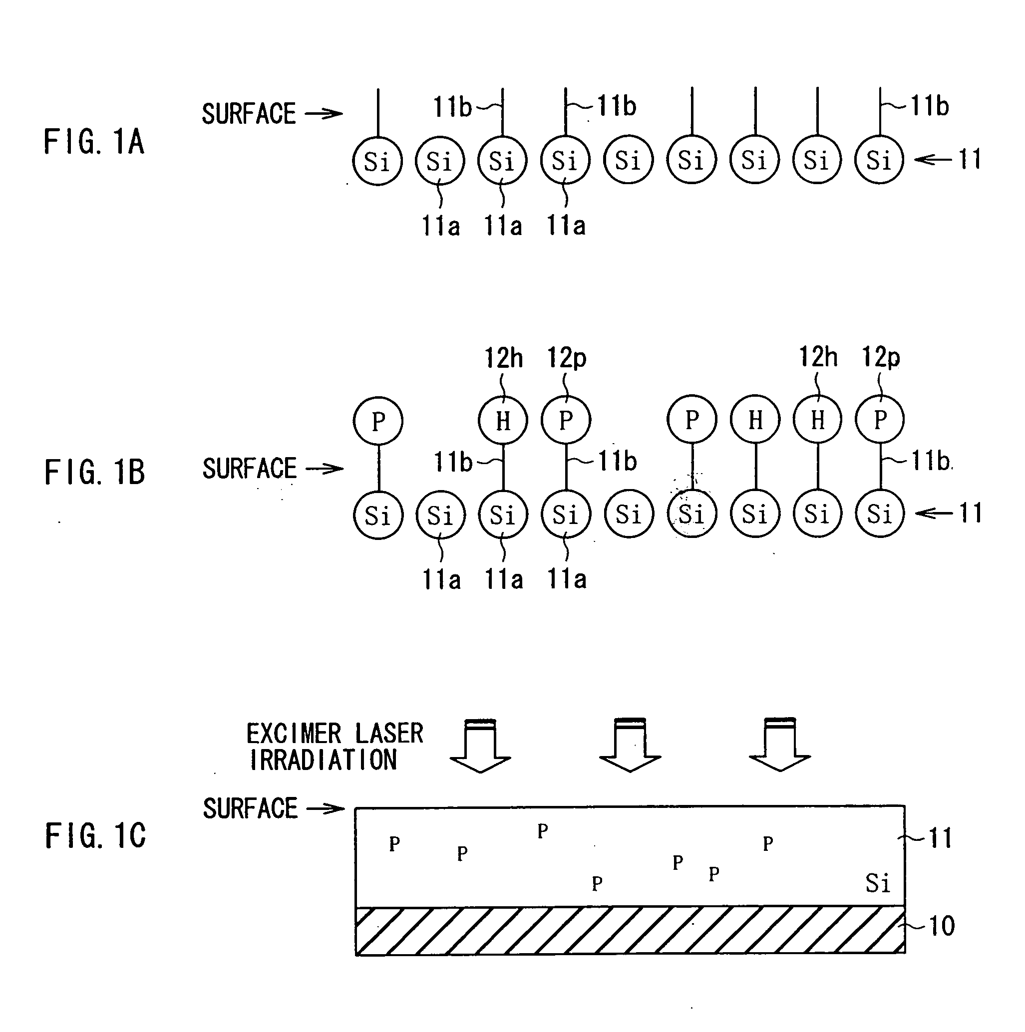
[0035] An embodiment of a method for doping a semiconductor layer according to the invention will be described in detail hereinbelow with reference to FIGS. 1A to 1C. The method for doping the semiconductor layer of the embodiment can form a low concentration impurity diffusion region in a silicon layer formed on a low heat resistant insulating substrate such as plastic or the like with good controllability.

[0036] First, as shown in FIG. 1A, a silicon layer 11 as a semiconductor layer is formed on an insulating substrate 10 (refer to FIG. 1C) and is crystallized by laser beam irradiation of excimer laser at this time. In the surface of the silicon layer 11, a lot of silicon atoms 11a exist in microcrystalline form and dangling bonds 11b exist in some of the silicon atoms 11a.

[0037] Next, as shown in FIG. 1B, dopant gas ion is adsorbed to terminate the dangling bonds 11b on the surface of the silicon layer 11 by plasma of dopant gas without semiconductor deposition gas. The dopant ...


PUM

PropertyMeasurementUnit
lengthsaaaaaaaaaa
deformation temperatureaaaaaaaaaa
temperatureaaaaaaaaaa

Abstract

A low concentration impurity diffusion region is formed with good controllability even in case of using a low heat resistant substrate. When doping a semiconductor layer, after forming the semiconductor layer on the substrate, the amount of the dopant ion adsorbed on a surface of the semiconductor layer is controlled by introducing hydrogen gas at the time of plasma irradiation and activating the adsorbed dopant ion in the semiconductor layer by an excimer laser.

Description

RELATED APPLICATION DATA [0001] This application is a divisional of co-pending application Ser. No. 10 / 433,849 filed Dec. 15, 2003, incorporated herein to the extent permitted by law. The present and foregoing applications claim priority to Japanese Application No. P2000-373052 filed on Dec. 7, 2000, and PCT Appliation No. PCT / JP01 / 10726 filed Dec. 7, 2001.BACKGROUND OF THE INVENTION [0002] The present invention relates to a method for doping a semiconductor layer, a method for manufacturing a thin film semiconductor device, method for controlling resistance of a semiconductor layer, and a thin film semiconductor device, and more particularly, a doping method using a crystallized semiconductor layer by excimer laser anneal, a method for manufacturing a thin film semiconductor device such as a thin film transistor, a thin film semiconductor device in which a semiconductor layer made of such as polycrystalline silicon is used as a channel. [0003] With progress of an advanced informati...

Claims


Application Information

Patent Timeline
Patent Type & Authority Applications(United States)
IPC IPC(8): H01L29/76G02F1/136G02F1/1368H01L21/20H01L21/223H01L21/225H01L21/265H01L21/268H01L21/336H01L21/77H01L21/84H01L29/786
CPCH01L21/223H01L21/2236H01L29/78621H01L21/268H01L29/66757H01L21/2254H01L29/786
Inventor MACHIDA, AKIOUSUI, SETSUOGOSAIN, DHARAM PAL
Owner MACHIDA AKIO
Why Eureka
Try Eureka