Stacked chip package with exposed lead-frame bottom surface

Inactive Publication Date: 2006-02-09
ULTRATERA
View PDF4 Cites 2 Cited by
  • Summary
  • Abstract
  • Description
  • Claims
  • Application Information

AI Technical Summary

Benefits of technology

[0011] Therefore, a primary object of the present invention is to provide a structure of a stacked chip package with exposed lead-frame bottom surface, in which the die supporting section of the lead-

Problems solved by technology

However, as the development of technology, various advanced portable devices such as laptop, mobile phone, personal digital assistants (PDAs), that are compact and light, require even smaller chips.
Due to the limitation of the component density per unit area, it would be hard to shrink the dimension of an individual IC chip.
Although various prior stacked chip structures are developed and known, and they are indeed effective in shrinking the dimension of the IC package, they ar

Method used


Image

  • Stacked chip package with exposed lead-frame bottom surface
  • Stacked chip package with exposed lead-frame bottom surface
  • Stacked chip package with exposed lead-frame bottom surface

Examples


first embodiment

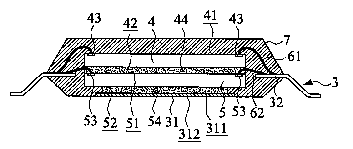
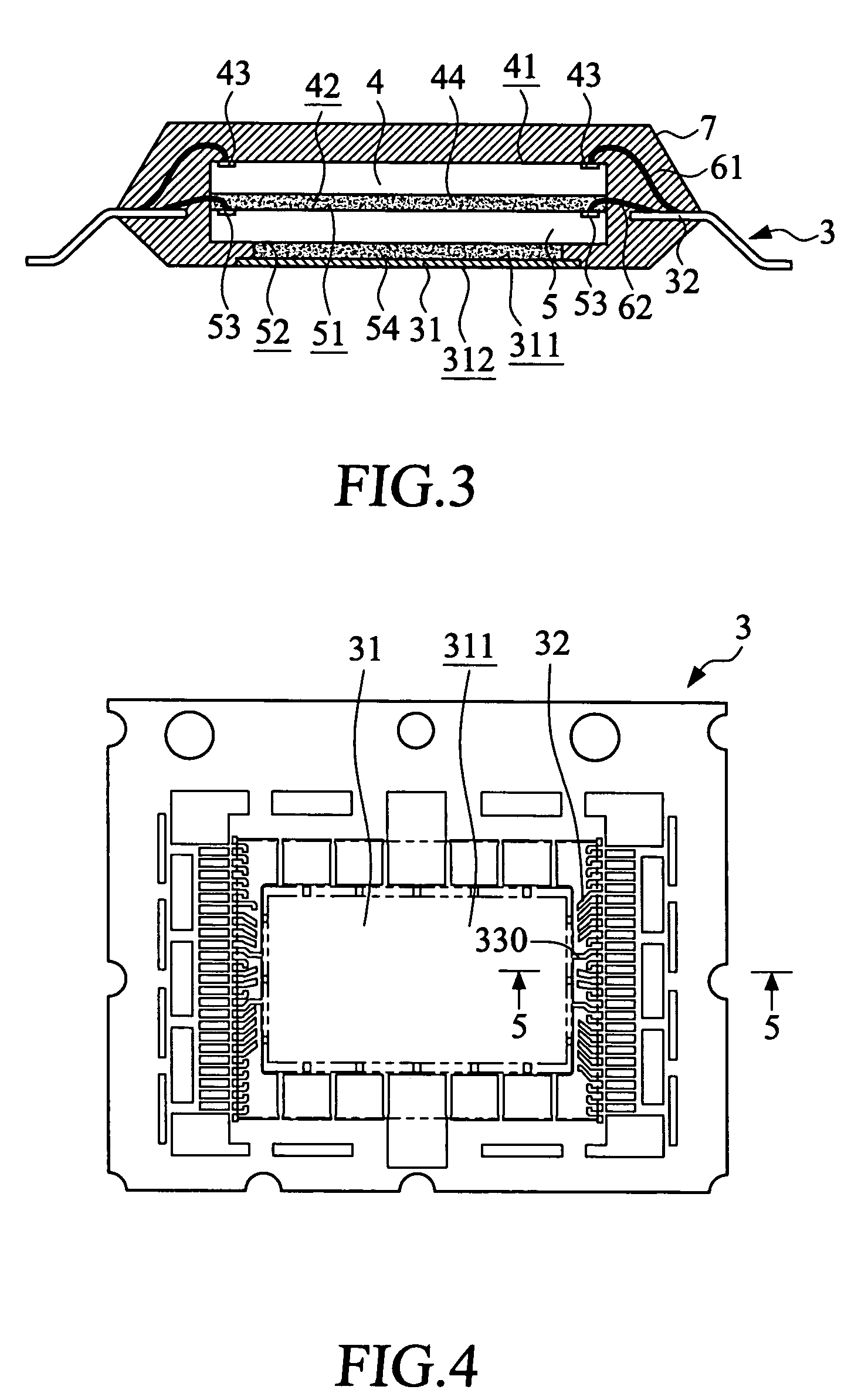
[0028] Referring to FIG. 3, a cross sectional view of a stacked chip package according to the present invention is shown. It shows that the stacked chip package comprises a lead-frame 3 which includes a die supporting section 31 and a plurality of lead fingers 32.

[0029]FIG. 4 is a top plan view of the lead-frame 3 of FIG. 3, and FIG. 5 is a cross sectional view taken along line 5-5 of FIG. 4. The die supporting section 31 of the lead-frame 3 is adapted to support and bear a die mounted thereon, which has a top surface 311 and a bottom surface 312. Each lead finger 32 is extended in a direction from the lead-frame 3 toward the die supporting section 31. The die supporting section 31 of the lead-frame 3 vertically deviates from the lead fingers 32 with a distance, forming an offset section 330 therebetween.

[0030] The stacked chip package comprises a first die 4 having an active surface 41 and a bottom surface 42. A plurality of die pads 43 are disposed on the active surface 41. Also,...

second embodiment

[0038] Referring to FIG. 7, a top plan view of the lead-frame 3 according to the present invention is shown. FIG. 8 is a cross sectional view taken along line 8-8 of FIG. 7.

[0039] In the design of the lead fingers 32 according to the second embodiment of the present invention, a first lateral section 331 of the lead fingers 32 is extended from the lead finger 32 toward the first die 4 and the second die 5. A bonding wire 61 interconnects the top of the first lateral section 331 to a corresponding die pad 43 disposed on an active surface 41 of the first die 4.

[0040] Moreover, a bent section 332 is extended from an inner end of the first lateral section 331 toward the second die 5, forming a deflected structure biasing to the second die 5. Then, a second lateral section 333 is extended from the inside end of the bent section 332, and the free end of the second lateral section 333 is stretched out close to the position of the second die 5. A bonding wire 62 interconnects a top of the ...


PUM


Abstract

A stacked chip package with exposed lead-frame bottom surface is disclosed. The stacked chip package includes a first die encapsulated in an encapsulated molding compound, which is mounted on an active surface of a second die. A bottom surface of the second die is mounted to a top surface of a die supporting section of the lead-frame. The bottom surface of the die supporting section is exposed outside the encapsulated molding compound. A plurality of bonding wires electrically interconnect the die pads of the first die and the second die to the corresponding lead fingers. Moreover, each lead finger of the lead-frame is preferably formed with a deflected structure with a bent section, which enables the dimension size of the stacked chip package to get more compact.

Description

BACKGROUND OF THE INVENTION [0001] 1. Field of the Invention [0002] The present invention relates to a stacked chip package, and more particularly to a compact structure of the stacked chip package with an exposed lead-frame bottom surface. [0003] 2. Description of the Prior Art [0004] Integrated circuit chips are widely applied in many electronic equipment, computer systems, and instruments. Integrated circuit chip is compact and can fit in small space. By applying chips, the dimensions of conventional electronic equipment can be largely reduced. However, as the development of technology, various advanced portable devices such as laptop, mobile phone, personal digital assistants (PDAs), that are compact and light, require even smaller chips. Practically, the dimension of chip is a critical factor to the design of many portable devices. [0005] In general, to shrink the dimension of an IC chip or to stack the IC chips to form a stacked chip package can meet the demand for more compac...

Claims


Application Information

Patent Timeline
IPC IPC(8): H01L23/48
CPCH01L23/49551H01L2924/01033H01L24/33H01L2224/32014H01L2224/32145H01L2224/32245H01L2224/48091H01L2224/48247H01L2224/73265H01L2924/01027H01L2924/01082H01L2924/14H01L23/49575H01L24/48H01L2924/00014H01L2924/181H01L2924/00012H01L2224/45099H01L2224/45015H01L2924/207
Inventor TSAI, MING-SUNGKIM, JIN-HOJANG, EUL-CHUL
Owner ULTRATERA
Why Eureka
Try Eureka