Supercharge Your Innovation With Domain-Expert AI Agents!

Semiconductor package, method for fabricating the same, and semiconductor device

a semiconductor and package technology, applied in the direction of semiconductor devices, semiconductor/solid-state device details, electrical apparatus, etc., to achieve the effects of preventing peeling of molding resin, enhancing adhesive properties between molding resin forming encapsulant and lead, and enhancing reliability of semiconductor packag

Inactive Publication Date: 2006-02-09
PANASONIC CORP
View PDF4 Cites 12 Cited by
  • Summary
  • Abstract
  • Description
  • Claims
  • Application Information

AI Technical Summary

Benefits of technology

[0010] An object of the present invention is to provide a semiconductor package with high reliability, a method for fabricating the semiconductor package, and a semiconductor device by taking measures to improve adhesivity of the leads of the semiconductor package to the resin.
[0012] With this configuration, adhesivity between a molding resin forming the encapsulant and the leads is improved, which prevents water or moisture from entering between the leads and the molding resin and prevents peeling-off of the molding resin. As a result, the reliability of the semiconductor package can be enhanced.
[0013] When the metal oxide film has a thickness of 10 nm or less, the aforementioned effect can be achieved while the efficiency in a plating process of the leadframe can be kept high.

Problems solved by technology

In the conventional semiconductor packages, it is known that due to insufficient adhesive strength between leads and a resin, the resin is peeled off from the leads and water or moisture enters the inside of the semiconductor packages through bonded surfaces, or breakage chips resulting from partial peeling-off of the resin enter equipments or semiconductor devices during the fabrication, leading to various disadvantages.

Method used


Image

  • Semiconductor package, method for fabricating the same, and semiconductor device
  • Semiconductor package, method for fabricating the same, and semiconductor device
  • Semiconductor package, method for fabricating the same, and semiconductor device

Examples


Embodiment Construction

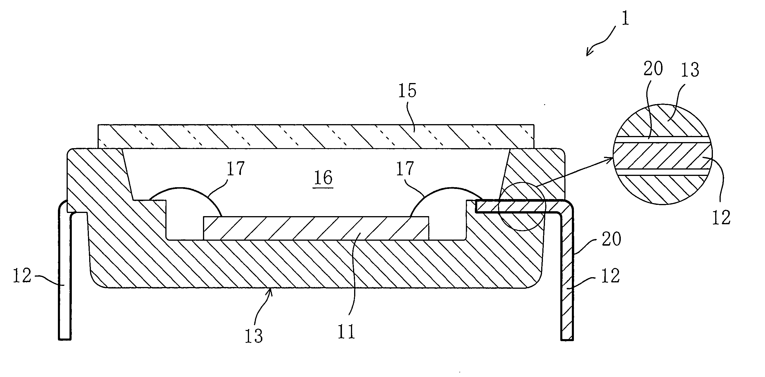
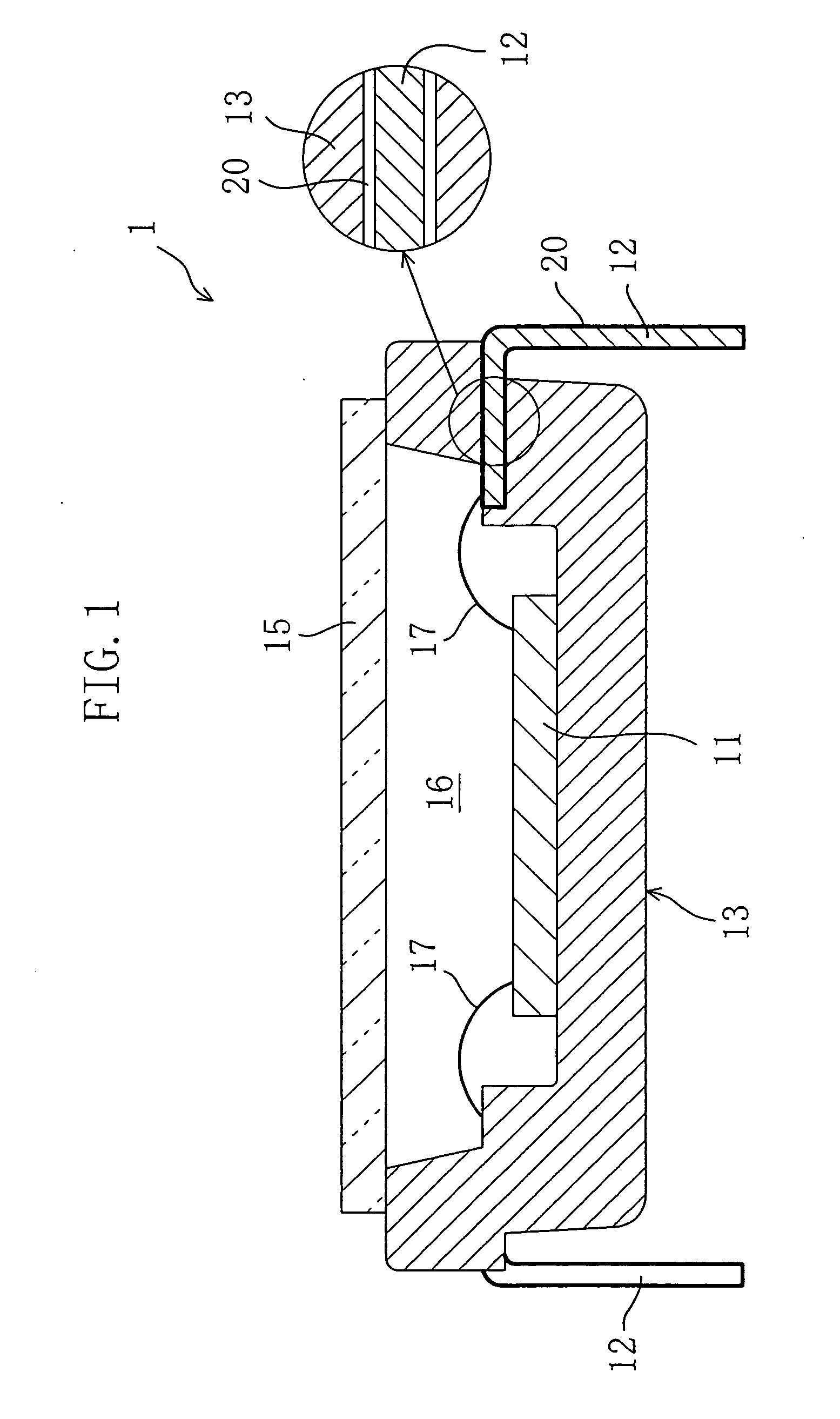
[0027]FIG. 1 is a cross sectional view illustrating the configuration of a semiconductor device 1 according to an embodiment of the present invention. The left end of FIG. 1 shows a cross section of a resin portion between leads, and the right end of FIG. 1 shows a cross section of a lead. As shown in FIG. 1, the semiconductor device 1 includes: a semiconductor chip 11 such as a solid-state imaging element, a light receiving / emitting element or an LSI; leads 12 for sending and receiving signals between the semiconductor chip 11 and an external device; fine metal wires 17 as electrically connecting members for connecting the semiconductor chip 11 to the leads 12; a rectangular dished encapsulant 13 for sealing the leads 12; and a lid member 15 such as a glass window or a hologram which is attached to the top surface of the encapsulant 13. The encapsulant 13 is formed in one piece from an epoxy resin poured during molding.

[0028] Moreover, the lid member 15 is attached to the top surf...


PUM


Abstract

A semiconductor device includes a semiconductor chip, leads for sending and receiving signals between the semiconductor chip and an external device, fine metal wires, an encapsulant for sealing the leads, and a lid member. On the surface of each of the leads, a metal oxide film is formed by an oxidation treatment. The metal oxide film has a thickness larger than a natural oxide film and no more than 80 nm.

Description

CROSS-REFERENCE TO RELATED APPLICATIONS [0001] The present application claims priority under 35 USC 119(a) to Japanese Patent Application No. 2004-230718 filed on Aug. 6, 2004 the entire contents of which are hereby incorporated by reference. BACKGROUND OF THE INVENTION [0002] (a) Field of the Invention [0003] The present invention relates to a semiconductor package which is equipped with an LSI chip, a solid-state imaging element, a light receiving / emitting element or the like and is made of a resin, a method for fabricating the same, and a semiconductor device. [0004] (b) Description of Related Art [0005] Conventionally, a typical molding of a semiconductor package has been carried out by sandwiching a leadframe having leads, dam bars that couple the leads to each other and other components between respective regions of upper and lower parts of a molding die adjacent to its die cavity, pouring a resin in the die cavity, and then curing the resin. [0006]FIG. 9 shows a cross section...

Claims


Application Information

Patent Timeline
Patent Type & Authority Applications(United States)
IPC IPC(8): H01L23/02
CPCH01L23/3142H01L24/48H01L23/49861H01L31/0203H01L2224/48091H01L2224/48247H01L2924/01025H01L2924/01078H01L2924/01079H01L2924/15153H01L2924/15165H01L2924/16195H01L23/49586H01L2924/00014H01L2224/451H01L24/45H01L2924/14H01L2924/00015H01L2924/00H01L23/28H01L23/52
Inventor INAO, HISAHOHIRANO, TATSUYASHIMIZU, KATSUTOSHI
Owner PANASONIC CORP
Features
  • R&D
  • Intellectual Property
  • Life Sciences
  • Materials
  • Tech Scout
  • Unparalleled Data Quality
  • Higher Quality Content
  • 60% Fewer Hallucinations
Learn More