Semiconductor device having low-K insulating film

a technology of insulating film and semiconductor, which is applied in the direction of basic electric elements, chemical vapor deposition coating, coating, etc., can solve the problems of affecting the practical application of the device, affecting the adhesion of the organic siloxane film b>8/b> and the dielectric protection film b>10/b> formed thereon, and achieving high adhesion. , the effect of improving the adhesion between the modified layer and

Inactive Publication Date: 2005-06-07
RENESAS ELECTRONICS CORP
View PDF7 Cites 4 Cited by
  • Summary
  • Abstract
  • Description
  • Claims
  • Application Information

AI Technical Summary

Benefits of technology

[0026]Further, when the dielectric protection film is formed by an aromatic polymer film, high adhesivity can be obtained. For example, in the step of forming wirings, for example, by a dual damascene method, when the organic siloxane film is formed as the dielectric film of the inter-level connection layer, and then the modified layer of the invention is formed and an aromatic polymer film is formed as the dielectric film for the wiring layer, adhesivity between the modified layer and the aromatic polymer film can be improved.

Problems solved by technology

However, the organic siloxane film involves a problem that adhesivity with a dielectric film at the upper layer is extremely low, which hinders practical application.
However, adhesivity between the organic siloxane film 8 and the dielectric protection film 10 formed thereon is generally poor and delamination tends to occur during a CMP step or the like as shown at a delamination portion 22 in FIG.
Such delamination results in deterioration of the reliability of wirings and lowering of the yield in the wiring steps.
However, since carbon is greatly decreased in the modified layer, the modified layer has high hygroscopicity.
As a result, this results in a problem of increasing the dielectric constant and also increasing the effective capacitance between wirings.
It is considered that a similar problem will occur even when water is used as an active gas.
Such a process is not effective for the improvement of the adhesivity.
This is because the fluorocarbon type polymer deposits on the organic siloxane film to rather lower the adhesion strength.
Therefore, even if the dielectric constant is lowered by the plasma treatment of using the gas described above, the dielectric constant cannot be recovered to the same value as in the original organic siloxane film.

Method used


Image

  • Semiconductor device having low-K insulating film
  • Semiconductor device having low-K insulating film
  • Semiconductor device having low-K insulating film

Examples


embodiment 1

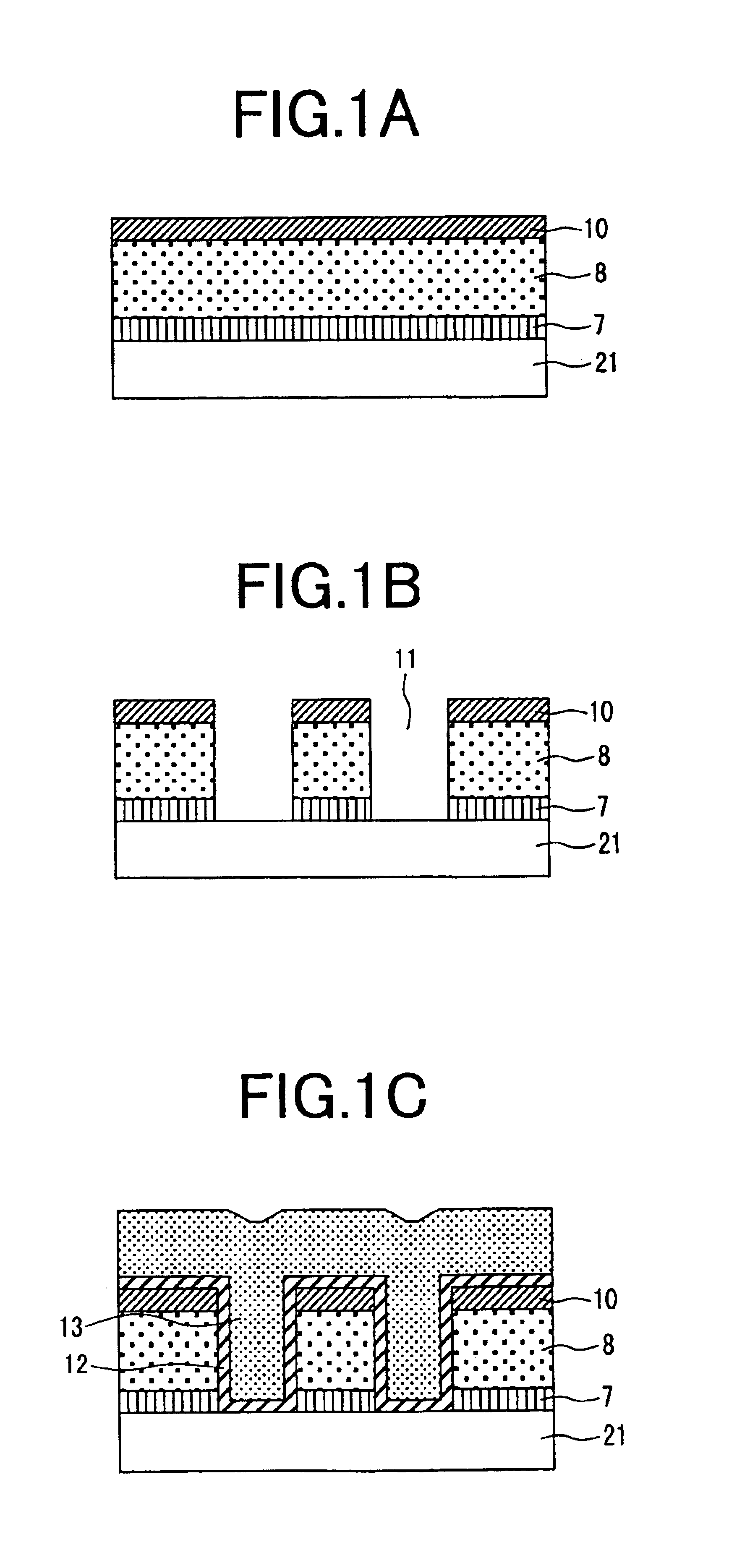
[0063]FIG. 3 shows a cross sectional view of a stacked structure in a first embodiment of the invention. An organic siloxane film 8, a modified layer 9 of the invention and a dielectric protection film 10 are formed in this order on a silicon substrate 1.

[0064]As the organic siloxane film 8, LKD manufactured by JSR Co., HSG manufactured by Hitachi Chemical Co., HOSP manufactured by Honeywell Co. obtained by a spin coating method, or Black Diamond manufactured by Applied Materials, Inc. and Coral manufactured by Novellus Systems, Inc. obtained by a CVD method was used. The thickness of the organic siloxane film 8 was 100 to 500 nm.

[0065]The modified layer 9 of the invention was formed by a plasma treatment using one of NF3, SF6, F2, CF4, CHF3, C2F6, or C4F8, or a plurality of gases mixed together in a plasma CVD apparatus. The conditions for the plasma treatment were gas flow rate of 10 to 2000 sccm, a pressure of 0.1 to 10 Torr, a temperature of 200 to 400° C. and an RF power of 250...

embodiment 2

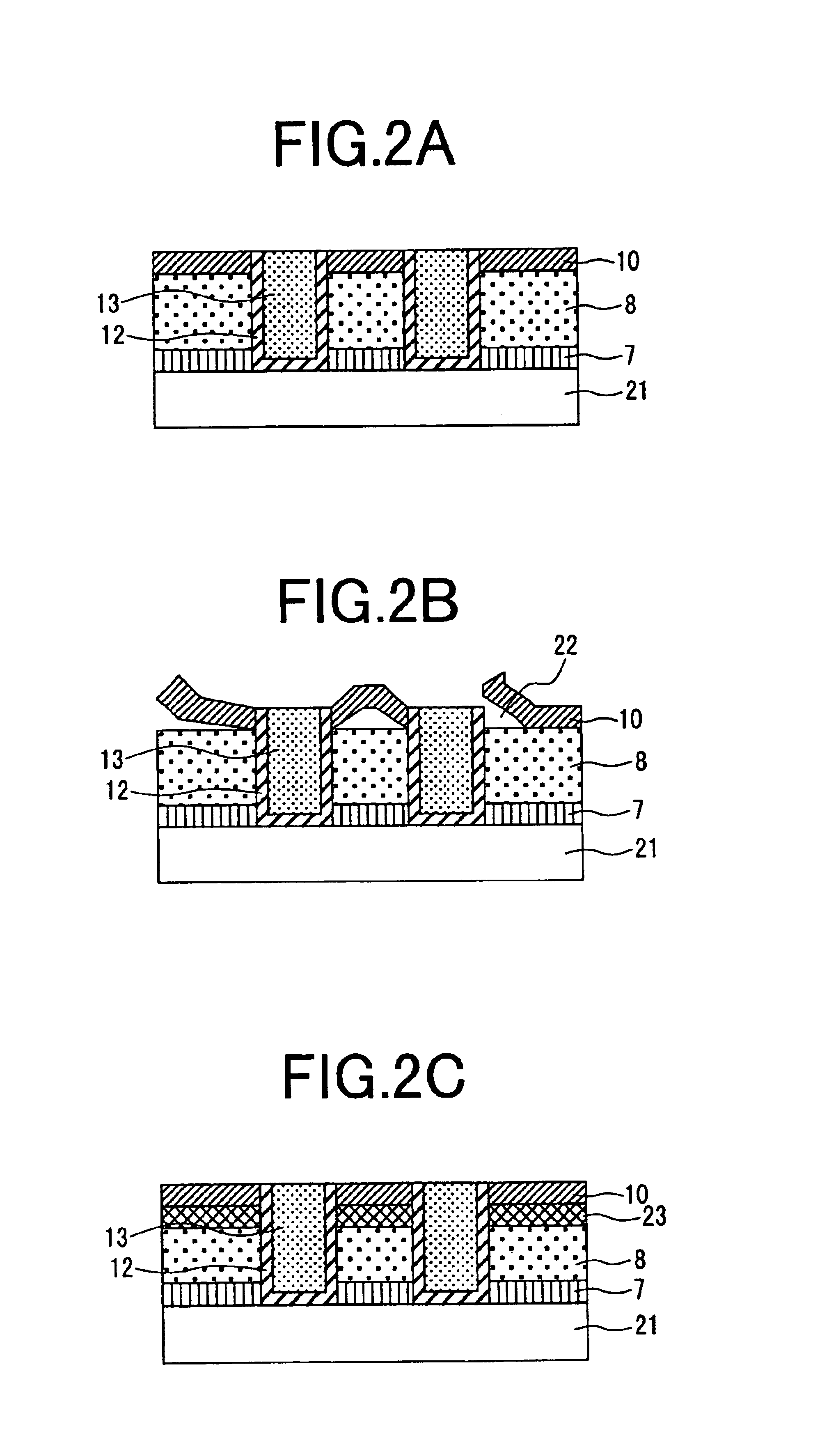
[0075]Multi-layered wirings of a semiconductor device were prepared by a copper damascene method. Embodiment 2 is to be described with reference to FIGS. 9 to 13.

[0076]In FIG. 9A, a transistor comprising an impurity diffusion layer 3 and a gate electrode 4 surrounded with an element isolation structure 2 is present on the surface of a silicon substrate 1. Further, a first inter-level dielectric layer 5 is formed so as to cover the transistor and a contact plug 6 is connected with the impurity diffusion layer 3 for electric conduction with the upper layer.

[0077]The first layer wirings were formed by a single damascene method as described below.

[0078]After depositing a second inter-level dielectric film 7 of 20 nm thickness as an etching stopper, an organic siloxane film 8 of 200 nm thickness was deposited. Further, a modified layer 9 of the invention was formed on the surface of the organic siloxane film under the condition shown in Embodiment 1. Successively, a dielectric protection...

embodiment 3

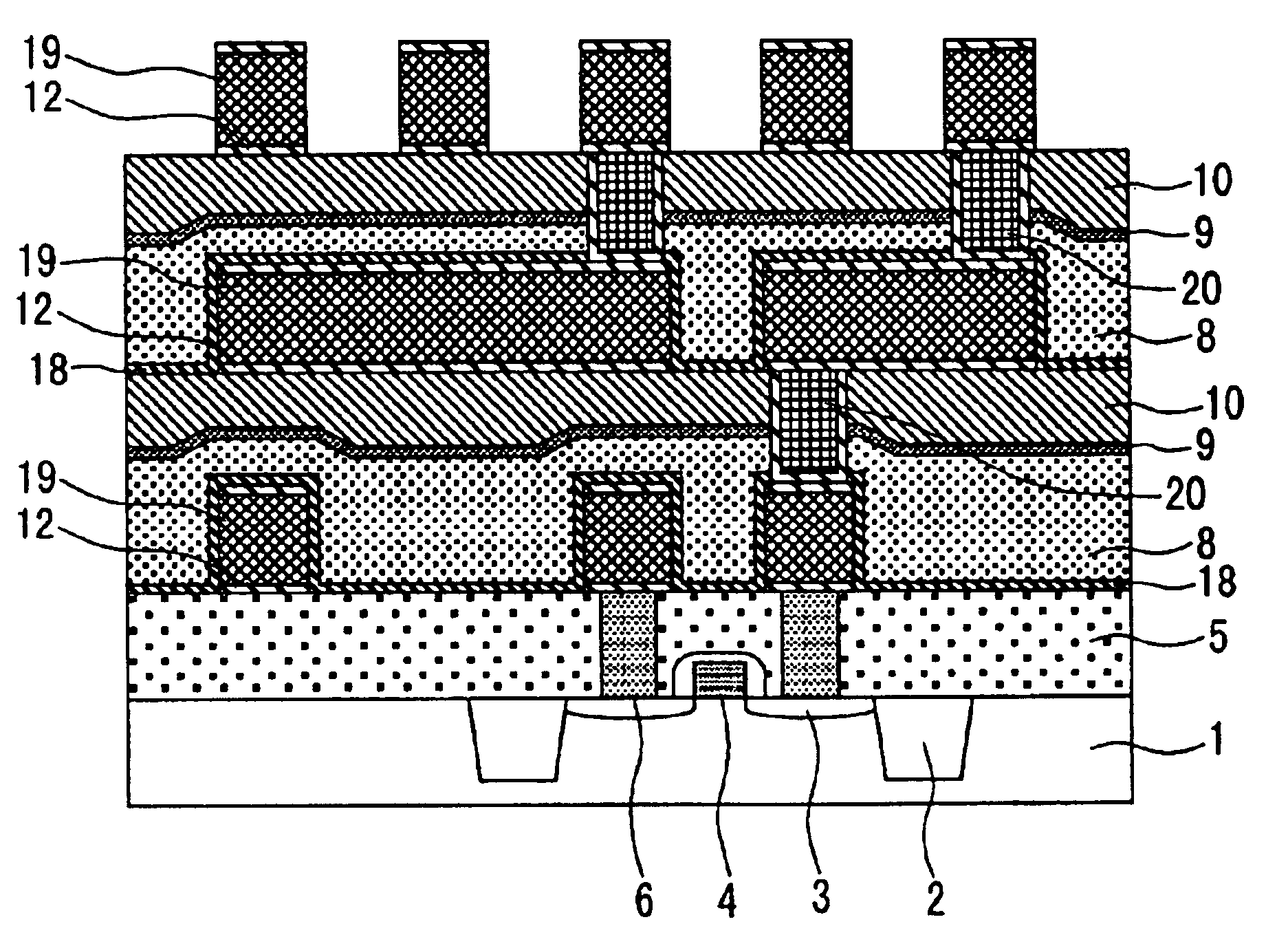
[0093]Multi-layered wirings for a semiconductor device were prepared by dry etching of an aluminum alloy by using the method of Embodiment 1. Embodiment 3 is to be described with reference to FIGS. 15 to 19.

[0094]As shown in FIG. 15A, on a silicon substrate 1, were formed an element isolation structure 2, an impurity diffusion layer 3, a gate electrode 4, a first inter-level dielectric film 5 and a contact plug 6. A barrier metal 12 of 30 nm thickness, an aluminum alloy film 19 of 250 nm thickness, and a barrier metal 12 of 30 nm thickness were formed on them in this order by a sputtering method. A titanium nitride film was used as the barrier metal film 12. After fabricating the metal films by using a resist pattern and dry etching, the resist was removed to form first layer wirings. Successively, a third inter-level dielectric film 18 of 30 nm thickness and an organic siloxane film 8 of 400 nm thickness were deposited so as to cover the first layer wirings. Further, a modified lay...


PUM

PropertyMeasurementUnit
dielectric constantaaaaaaaaaa
thicknessaaaaaaaaaa
thicknessaaaaaaaaaa

Abstract

Disclosed is a semiconductor device having a dielectric film of a stacked structure, comprising a low dielectric constant film containing silicon, oxygen and carbon a modified layer for the low dielectric constant film containing silicon, oxygen, carbon and fluorine and a dielectric protection film formed successively on a semiconductor substrate, the semiconductor device being manufactured by applying a plasma treatment using a fluorine-containing gas to the surface of an organic siloxane film to form a modified layer and then forming a dielectric protection film, which can improve the adhesivity with the dielectric protection film without increasing the dielectric constant of the organic siloxane film to prevent delamination.

Description

[0001]This is a divisional application of U.S. Ser. No. 10 / 414,010, filed Apr. 16, 2003, now U.S. Pat. No. 6,777,325.BACKGROUND OF THE INVENTION[0002]1. Field of the Invention[0003]The present invention relates to a semiconductor device and a manufacturing method thereof and more particularly to a semiconductor device at high integration degree and of high speed operation, and a manufacturing method thereof.[0004]2. Description of the Related Art[0005]In recent years, with a view point of increasing the integration degree and the operation speed of semiconductor devices, decrease in the inter-wiring capacitance has been required. Then, studies have been made vigorously for introducing dielectric films of lower dielectric constant than existent silicon oxide films (dielectric constant: 3.9-4.2) as inter-wiring dielectric films (hereinafter simply referred to as low dielectric constant films).[0006]Typical low dielectric constant films of dielectric constant of 3 or less can include, ...

Claims


Application Information

Patent Timeline
Patent Type & Authority Patents(United States)
IPC IPC(8): H01L23/52H01L23/48H01L29/40H01L21/312H01L21/316H01L21/4763H01L23/522H01L21/768H01L31/0328
CPCC23C16/0272H01L21/7684H01L21/02126H01L21/02131H01L21/022H01L21/02216H01L21/02282H01L21/02321H01L21/0234H01L21/02362H01L21/3122H01L21/31629H01L21/31633H01L21/76801H01L21/76807H01L21/76819H01L21/76822H01L21/76826H01L21/76829H01L21/76832H01L21/76835C23C16/401H01L21/312H01L21/3143H01L21/3148H01L21/3185
Inventor RYUZAKI, DAISUKEFURUSAWA, TAKESHI
Owner RENESAS ELECTRONICS CORP
Why Eureka
Try Eureka