Multi-layer board manufacturing method

Inactive Publication Date: 2006-03-02
DENSO CORP
View PDF6 Cites 31 Cited by
  • Summary
  • Abstract
  • Description
  • Claims
  • Application Information

AI Technical Summary

Benefits of technology

[0021] Under this manufacturing method, before a chip component is inserted into a via hole, the resin-film pile is heated and pressed so that each resin film of the pile temporary adheres and is fixed to each other. As a res

Problems solved by technology

The chip component may therefore deviate from a preset position, enter into an interval space between the piled films, or jump up o

Method used


Image

  • Multi-layer board manufacturing method
  • Multi-layer board manufacturing method
  • Multi-layer board manufacturing method

Examples


Example

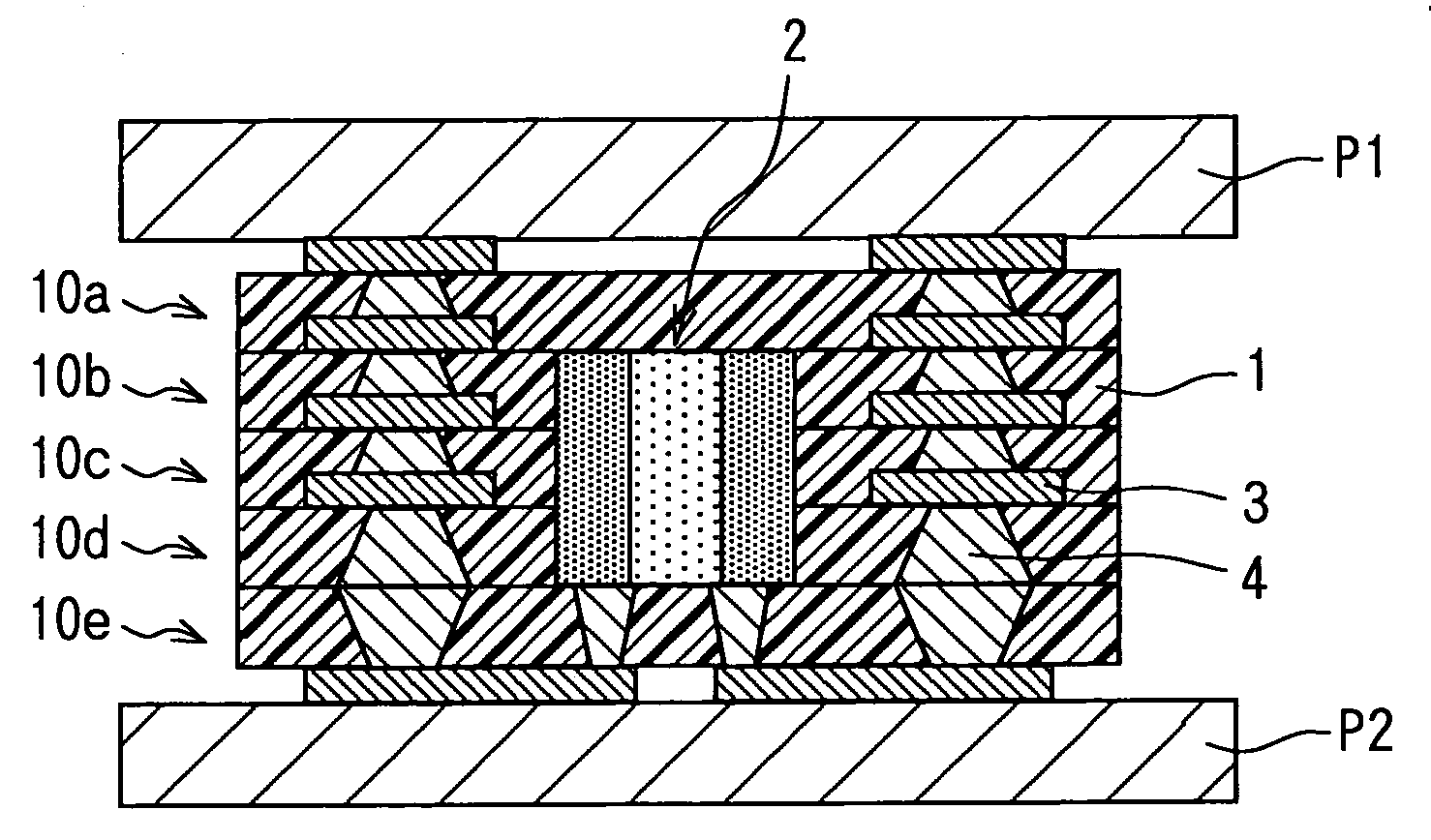
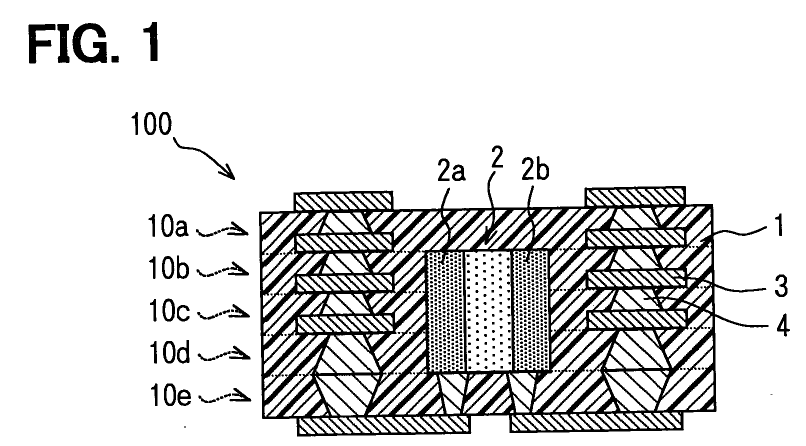
[0028]FIG. 1 shows a schematic sectional view of a multi-layer board 100 manufactured by a method according to an embodiment of the present invention. Here, a chip component 2 is shown with electrodes 2a, 2b formed on a surface of the chip component 2 being explicitly shown.

[0029] The multi-layer board 100 embeds the chip component 2 inside an insulating substrate (or base member) 1, which is formed by causing five resin films 10a to 10e (divided by dotted lines in FIG. 1) to adhere each other. Further, conductive patterns 3 are formed on some of the resin films 10a to 10e; each of the conductive patterns formed on the individual resin films 10a to 10e is electrically connected each other using conductive members 4 formed by sintering conductive pastes. The electrodes 2a, 2b of the chip component 2 are electrically connected to the conductive patterns 3 via the conductive members 4.

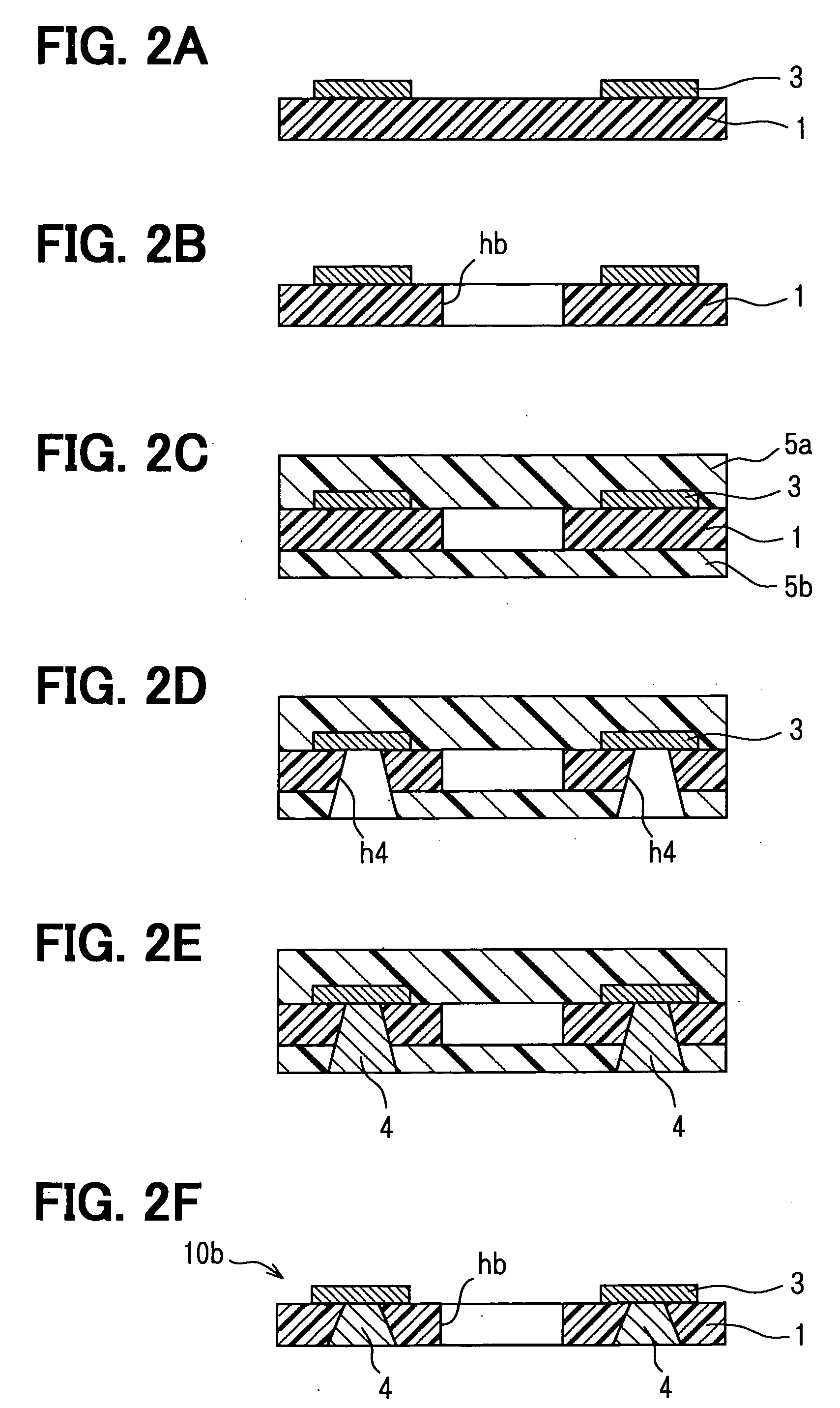
[0030] Next, a manufacturing method of the multi-layer board 100 will be explained below with refere...


PUM

PropertyMeasurementUnit
Lengthaaaaaaaaaa
Lengthaaaaaaaaaa
Angleaaaaaaaaaa

Abstract

Two types of resin films are prepared for manufacturing a multi-layer board containing a chip component. A fist type has a via hole for the chip component to be inserted into, while a second type does not have the via hole. Resin films including the two types are piled before the chip component is inserted. At least a given resin film of the first type has a via hole provided with protruding members. Of the protruding members, opposing protruding members form a gap between their tips. This gap is shorter than an outer dimension of the inserted chip component. The chip component crushes portion of the tips of the protruding members while being pressed and inserted into the via hole in the given resin film.

Description

CROSS REFERENCE TO RELATED APPLICATIONS [0001] This application is based on and incorporates herein by reference Japanese Patent Application No. 2004-254868 filed on Sep. 1, 2004. FIELD OF THE INVENTION [0002] The present invention relates to a manufacturing method of a multi-layer board where a chip component is embedded in an insulating substrate. BACKGROUND OF THE INVENTION [0003] Patent Document 1 describes a method of manufacturing a multi-layer board (printed circuit board) so that a chip component is embedded in an insulating substrate (or base member). Here, multiple single-sided conductive pattern resin films made of thermoplastic resin are provided with via holes. The via holes are disposed in positions corresponding to the embedded chip component (or electrical element) to have dimensions approximately equal to an outer dimension of the chip component. Then the multiple resin films are piled, and the chip component is inserted into a concave space (or hole) formed by the ...

Claims


Application Information

Patent Timeline
IPC IPC(8): H05K3/36
CPCH05K1/186Y10T29/49133H05K3/4614H05K3/4617H05K3/4632H05K2201/0129H05K2201/0141H05K2201/0394H05K2201/10636H05K2203/063Y10T29/49146Y10T29/49128Y10T29/49126Y10T29/49163Y10T29/49165Y10T29/49155H05K3/4069Y02P70/50H05K3/46
Inventor TAKEUCHI, SATOSHISHIMIZU, MOTOKI
Owner DENSO CORP
Why Eureka
Try Eureka