
Overlay control circuit and method

a control circuit and overlay technology, applied in static indicating devices, instruments, cathode-ray tube indicators, etc., can solve the problems of insufficient memory bandwidth to accommodate all demands in a timely manner, not all of the main image data is transmitted to the display, and the amount of memory bandwidth wasted can be significant, so as to reduce the memory bandwidth requirements and conserve power

Inactive Publication Date: 2006-03-02
SEIKO EPSON CORP
View PDF16 Cites 22 Cited by
  • Summary
  • Abstract
  • Description
  • Claims
  • Application Information

AI Technical Summary

Benefits of technology

[0009] Accordingly, there is a need for an overlay control circuit and method that reduces memory bandwidth requirements and conserves power.

Problems solved by technology

And when access to memory is required by many devices or large data transfers are required, the memory bandwidth may be insufficient to accommodate all demands in a timely manner.
However, not all of the main image data are transmitted to the display.
It is a problem of no small significance that main image data are fetched from memory for pixel locations in the display for which overlay image data is displayed.
It is a problem because image data are fetched, but not used.
But where main and overlay images are frequently rendered together on a display, the amount of memory bandwidth wasted can be significant.
Further, a significant amount of power can be wasted.
And in battery powered devices, power conservation is critical.

Method used


Image

  • Overlay control circuit and method
  • Overlay control circuit and method
  • Overlay control circuit and method

Examples


Embodiment Construction

[0024] The invention is directed to an overlay circuit and method for reducing memory bandwidth and power consumption requirements when displaying a main image overlaid by an overlay image. This specification describes the present preferred embodiments of the invention, examples of which are illustrated in the accompanying drawings. Whenever possible, the same reference numbers are used in the drawings and specification to refer to the same or like parts, blocks, and steps.

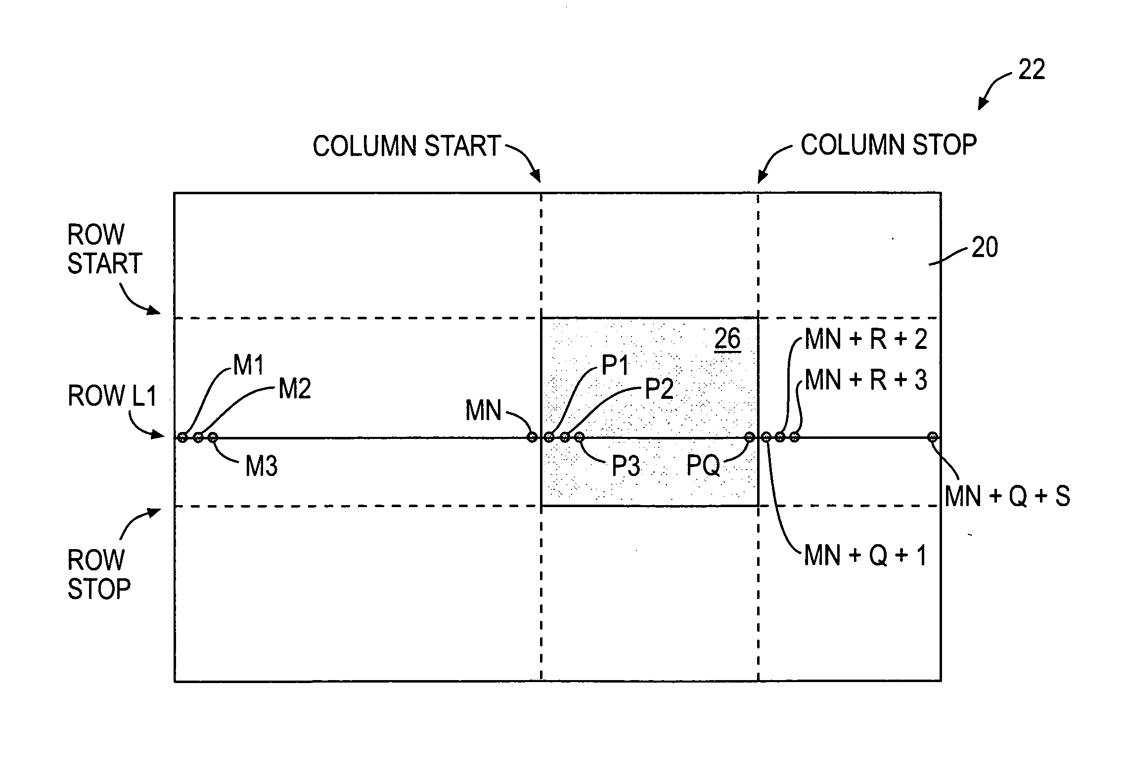
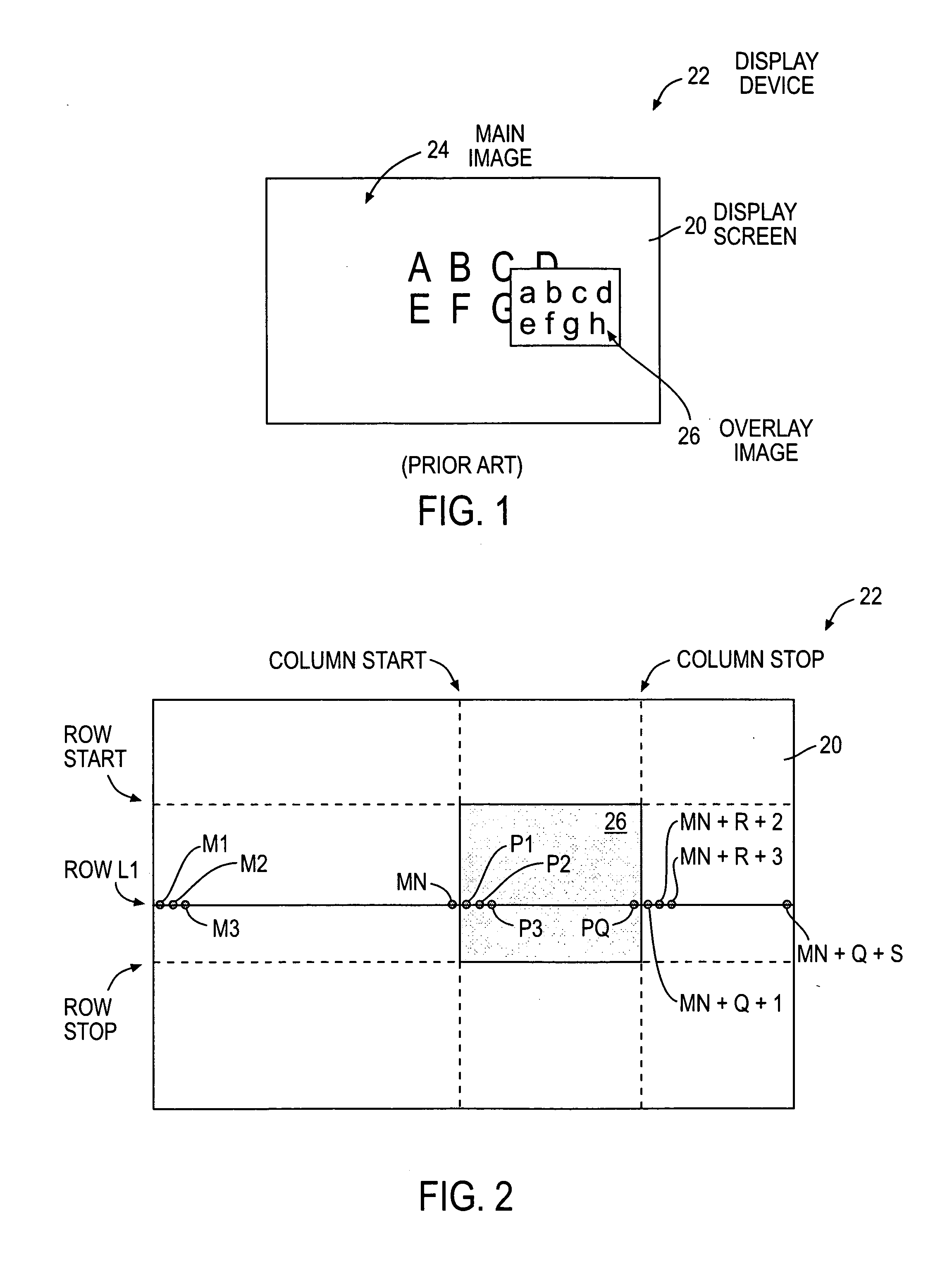
[0025]FIG. 1 shows a display screen 20 of a display device 22. The display device 22 is typically an LCD panel but may be any device capable of rendering image data, including CRT and OLED display devices, as well as hard copy rendering devices, such as printers. The screen 20 displays a main image 24. Often the main image 24 is coextensive with the area of the screen 20 for displaying main image data, though this is not necessary. The screen 20 may also include an overlay image 26 that is typically rectangular f...


PUM


Abstract

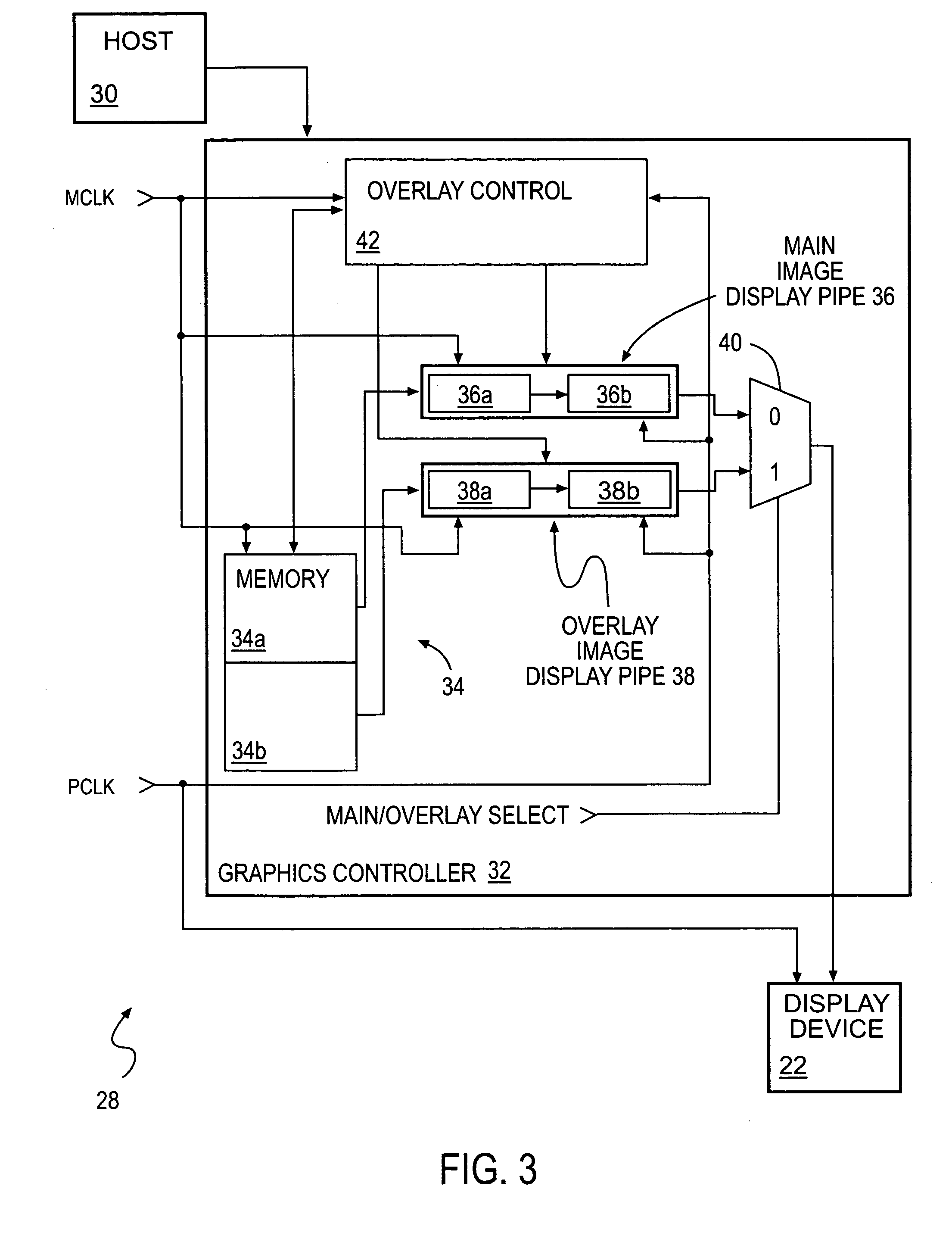
An overlay control circuit and method. In a preferred embodiment of the invention, a graphics controller provides main image data and overlay image data to a display device and includes a memory for storing the main image data and the overlay image data and a logic circuit for producing a signal that, in an active state, indicates that a particular location in the display device is to be represented by the overlay image data. The overlay control circuit fetches the main image data from the memory and is further adapted to respond to a transition in the indicating signal to the active state by halting the fetching.

Description

FIELD OF INVENTION [0001] The invention relates to digital image processing. More particularly, the invention is directed to an overlay circuit and method for reducing memory bandwidth and power consumption requirements when displaying a main image overlaid by an overlay image. BACKGROUND [0002] Digital images are comprised of arrays of pixels. A pixel is a discrete element in a display screen that can be illuminated with a particular color and degree of brightness. The term pixel is also used to refer to the datum that define the color and intensity of the physical pixels in display and hard copy rendering devices. [0003] Graphics display systems typically employ a graphics controller for controlling the flow of image data from a host processor or a peripheral device, such as a camera, to a display device such as an LCD. Commonly, graphics display systems are employed in all types of computer systems, including portable devices, such as cellular telephones, personal digital assista...

Claims


Application Information

Patent Timeline
Patent Type & Authority Applications(United States)
IPC IPC(8): G09G5/00
CPCG09G5/397
Inventor RAI, BARINDER SINGHSOROUSHI, ATOUSA
Owner SEIKO EPSON CORP
Learn More