

Optical device
a technology of optical devices and ridges, applied in the field of optical devices, can solve problems such as preventing stable optical control, and achieve the effect of reducing the stress applied on the second ridge section
- Summary
- Abstract
- Description
- Claims
- Application Information
AI Technical Summary
Benefits of technology
Problems solved by technology
Method used
Image

Examples
first embodiment
[A1] Explanation of First Embodiment
[A1-1] Structure of Optical Device 1 According to First Embodiment
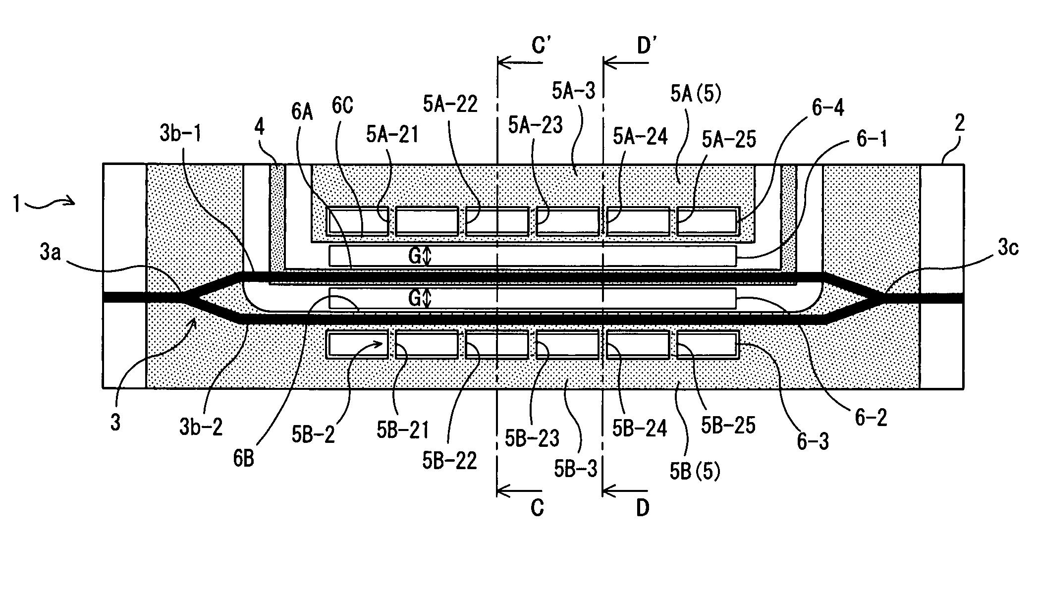
[0067]FIG. 1 is a schematic plane view showing an optical device 1 according to a first embodiment of the present invention. FIG. 2 is a sectional view of the optical device 1 shown in FIG. 1 when seen in the direction of arrows C and C′. FIG. 3 is a sectional view of the optical device 1 shown in FIG. 1 when seen in the direction of arrows D and D′. In the optical device 1 shown in FIG. 1, for example, a Mach-Zehnder type optical waveguide 3 is formed on a substrate 2 having an electrooptic effect made of LiNbO3 (lithium niobate, hereinafter, simply referred to as LN) and the like, by titanium diffusion or proton exchange, and a signal electrode 4 and a ground electrode 5 for applying an electric field to light transmitting through this optical waveguide 3 are formed. And the light transmitting through this optical waveguide 3 can be controlled by the electric field that the signa...
second embodiment
[B] Explanation of Second Embodiment
[B-1] Structure of Optical Device 20 According to Second Embodiment
[0103]FIG. 6 is a schematic plane view showing an optical device 20 according to a second embodiment of the present invention. The optical device 20 shown in FIG. 6, compared with the optical device 1 according to the first embodiment or the optical device 10 according to the modified example of the first embodiment, in the interaction regions, instead of the straight line waveguides 3b-1 and 3b-2, comprises a Mach-Zehnder type optical waveguide 13 having curved waveguides (first and second optical waveguides) 3d-1 and 3d-2, which have a curve of at least 90 degrees or more. Further, the optical device 20 comprises a signal electrode 14 and a ground electrode 15 having a pattern corresponding to a pattern of the curved waveguides 3d-1 and 3d-2. Above-mentioned points are different from the first embodiment. In this, in FIG. 6, the same reference number as that in FIGS. 1 to 3 show...
third embodiment
[C] Explanation of Third Embodiment
[C-1] Structure of Optical Device 30 According to Third Embodiment
[0113]FIG. 7 is a schematic plane view showing an optical device 30 according to a third embodiment of the present invention. FIG. 8 is a sectional view of the optical device 30 shown in FIG. 7 when seen in the direction of arrows F and F′. In the optical device 30 according to the third embodiment, compared with the optical device 1 according to the first embodiment, a forming pattern of a ground electrode 35 is different. In this, the structure except the ground electrode 35 is basically the same as the optical device 1 in the first embodiment, and in FIGS. 7 and 8, the same reference number as that in FIGS. 1 to 3 shows almost the same portion.
[0114] The ground electrode 35 comprises a first electrode portion 35A and a second electrode portion 35B, which were formed so as to sandwich the signal electrode 4 with a predetermined gap between the signal electrode 4 and each of the f...
PUM
| Property | Measurement | Unit |
|---|---|---|
| width | aaaaa | aaaaa |
| width | aaaaa | aaaaa |
| thickness | aaaaa | aaaaa |
Abstract
Description
Claims
Application Information