Manufacturing method for strained silicon wafer

a manufacturing method and silicon wafer technology, applied in the direction of basic electric elements, electrical apparatus, semiconductor devices, etc., can solve the problems of increasing junction leak current, generating uneven cross-hatching, and generating similar dislocations at high density, so as to reduce the degree of freedom in the device process, the effect of increasing the film thickness

Inactive Publication Date: 2006-03-16
COVALENT MATERIALS CORP
View PDF3 Cites 23 Cited by
  • Summary
  • Abstract
  • Description
  • Claims
  • Application Information

AI Technical Summary

Benefits of technology

[0027] By passing through these steps, the penetrating dislocation density in the strained Si layer can be more reduced and the strained Si layer can be formed to a thickness larger than the critical film thickness of a strained Si having a lattice constant corresponding to the maximum Ge concentration of the stain-relaxed SiGe layer.
[0028] In this way, by forming the Si1-yGey layer having a Ge concentration lower than the maximum Ge concentration in the Si1-xGex layer before the strained Si layer is formed, the critical film thickness of allowing for abrupt increase of the penetrating dislocation density can be made large and in turn, an Si layer reduced in the penetrating dislocation density and having a larger film thickness can be formed.
[0029] As described above, according to the present invention, the penetrating dislocation density in a strained silicon wafer can be more reduced relative to the conventional technique, and also, a strained layer having a larger film thickness can be formed.
[0030] The strained silicon wafer of the present invention has such a high-quality strained Si layer, so that when the strained Si layer is used as the device activity region, the degree of freedom in the device process can be elevated and high carrier mobility can be realized. Therefore, the strained silicon wafer of the present invention can be suitably used for LSI, a discrete semiconductor device and the like in or after the next generation.

Problems solved by technology

However, at the epitaxial growth of an SiGe layer on a silicon substrate, misfit dislocations are generated due to difference in the lattice constant between Si and SiGe, and penetrating dislocations attributable to the misfit dislocations reach the surface at a high density, which brings about a problem that dislocations similarly at a high density are generated also in the strained Si layer formed on the SiGe layer.
Dislocations in the strained Si layer give rise to increase in the junction leak current at the formation of a device element.
Furthermore, there arises a problem that unevenness called cross-hatch is generated on the strained Si layer surface due to penetrating dislocations and residual strain energy.
Such a high penetrating dislocation density may greatly affect the yield in the device process.

Method used


Image

  • Manufacturing method for strained silicon wafer
  • Manufacturing method for strained silicon wafer

Examples


examples

[0057] The present invention is described in greater detail below by referring to Examples, but the present invention is not limited to these Examples.

examples 1 to 6

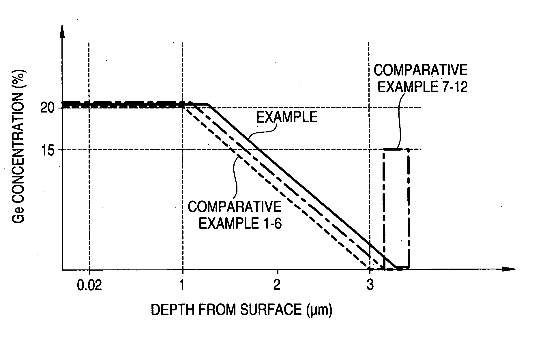
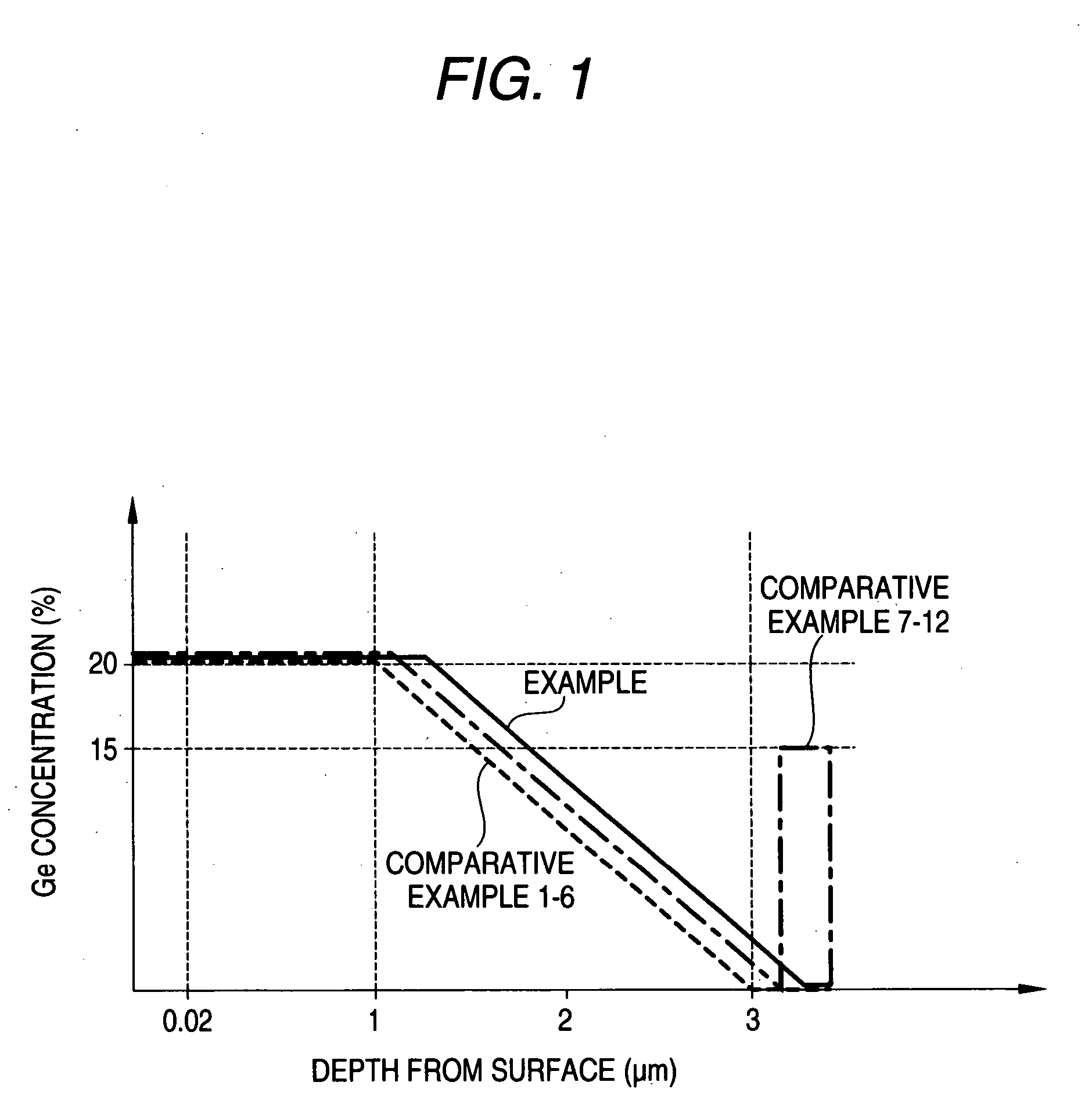
[0058] On the mirror-polished surface of a single crystal silicon substrate, an Si1-xGex composition-graded layer of which the Ge concentration x is varied in 10 steps within the range of 0≦x≦0.2 was epitaxially grown to a film thickness of 2 μm.

[0059] Subsequently, an Si0.8Ge0.2 uniform composition layer of which the Ge concentration is constantly 20% was epitaxially grown thereon as a strain-relaxing layer to a film thickness of 1 μm.

[0060] Furthermore, an Si0.85Ge0.15 uniform composition layer of which the Ge concentration is constantly 15% was epitaxially grown thereon to a film thickness of 20 nm.

[0061] Thereafter, on the surface of this layer, a strained Si layer was formed by changing the film thickness so as to prepare six samples of strained silicon wafers (Examples 1 to 6).


PUM

PropertyMeasurementUnit
thicknessaaaaaaaaaa
resistivityaaaaaaaaaa
thicknessaaaaaaaaaa

Abstract

A manufacturing method for producing a stained silicon wafer has the steps of forming an Si1-xGex composition-graded layer of which Ge concentration is stepwisely increased on a single crystal silicon substrate, forming an Si1-xGex uniform composition layer of which Ge concentration is constant on the Si1-xGex composition-graded layer, forming a stain-relaxed Si1-yGey layer of which Ge concentration y is constant while y satisfies relationship of 0.5x≦y<x on the Si1-xGex uniform composition layer and epitaxially growing a strained Si layer on the strain- relaxed Si1-yGey layer.

Description

[0001] The present invention claims foreign priority to Japanese patent application no. P.2004-262274, filed on Sep. 9, 2004, the contents of which is incorporated herein by reference. BACKGROUND OF THE INVENTION [0002] 1. Field of the Invention [0003] The present invention relates to a manufacturing method for a silicon wafer reduced in the penetrating dislocation density by stacking an SiGe layer and a strained Si layer on a silicon substrate. [0004] 2. Description of the Background Art [0005] In recent years, a stained silicon wafer obtained by epitaxially growing an SiGe layer on a single crystal silicon substrate and epitaxially growing a strained Si layer on the SiGe layer has been proposed. [0006] In the strained Si layer, a tensile strain is generated due to the SiGe layer having a large lattice constant as compared with Si. This generated strain causes a change in the band structure of Si to release the degeneracy. As a result, the carrier mobility increases. [0007] Accordi...

Claims


Application Information

Patent Timeline
Patent Type & Authority Applications(United States)
IPC IPC(8): H01L21/302
CPCH01L21/02381H01L21/0245H01L21/0262H01L21/0251H01L21/02532H01L21/02505H01L21/20
Inventor SENDA, TAKESHIIZUNOME, KOJI
Owner COVALENT MATERIALS CORP
Why Eureka
Try Eureka