Silicon carbide semiconductor device and method for manufacturing the same
- Summary
- Abstract
- Description
- Claims
- Application Information
AI Technical Summary
Benefits of technology
Problems solved by technology
Method used
Image

Examples
first embodiment
Mode
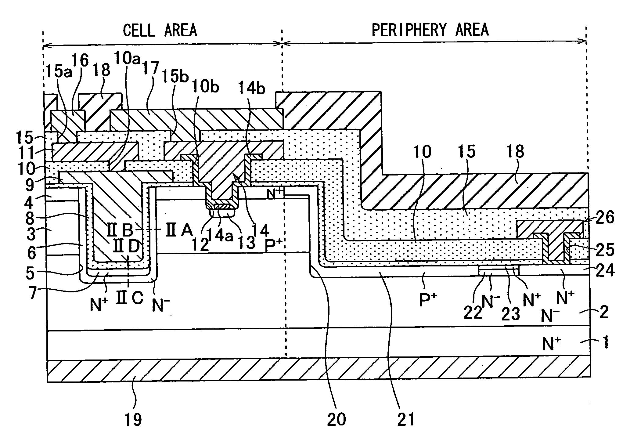
[0038]FIG. 1 shows the sectional construction of a vertical type power MOSFET of a trench type in a first embodiment mode of the present invention. The structure of the vertical type power MOSFET of this embodiment mode will next be explained with reference to this figure. In this figure, the left-hand side of the paper face shows the sectional construction of a cell area of the vertical type power MOSFET, and the right-hand side shows the sectional construction of an outer circumferential area as a periphery area.
[0039] As shown in FIG. 1, an N− type drift layer 2 is arranged on an N+ type substrate 1. A P+ type base area 3 and an N+ type source area 4 are formed on the surface of this N− type drift layer 2. In this embodiment mode, the N+ type substrate 1, the N− type drift layer 2, the P+ type base area 3 and the N+ type source area 4 provide a semiconductor substrate, and the cell area and the outer circumferential area are formed.
[0040] A trench 5 extending through the N+...
second embodiment
Mode
[0102] A second embodiment mode of the present invention will be explained. FIG. 23 shows the sectional construction of a vertical type power MOSFET of the trench type in this embodiment mode. The construction of the vertical type power MOSFET of this embodiment mode will next be explained with reference to FIG. 23.
[0103] In the vertical type power MOSFET of this embodiment mode, the N+ type substrate 1 having a surface set to an off plane of [11-20] is used, and the side wall face of the trench 5 is set to plane of (11-20).
[0104] As shown in FIG. 23, in the vertical type power MOSFET of this embodiment mode, the N+ type low resistance layer 7 is formed in a portion located on the bottom face of the trench 5 within the N− type channel layer 6 formed within the trench 5. However, a structure for partially deepening an area 7a of one portion of this N+ type low resistance layer 7 and reaching the most bottom face side of the N− type channel layer 6, i.e., reaching until the N− t...
third embodiment
Mode
[0126] A third embodiment mode of the present invention will be explained. FIG. 30 shows the sectional construction of a cell area of a vertical type power MOSFET of the trench type in this embodiment mode. The construction of the vertical type power MOSFET of this embodiment mode will next be explained with reference to FIG. 30. However, the basic construction of the third embodiment mode is similar to that of the above second embodiment mode.
[0127] As shown in FIG. 30, the sectional structure of the vertical type power MOSFET of this embodiment mode is similar to that of the vertical type power MOSFET of the second embodiment mode. However, N type impurities, P type impurities, or a SiC raw material not set to impurities is implanted as atoms into the oxide film 8.
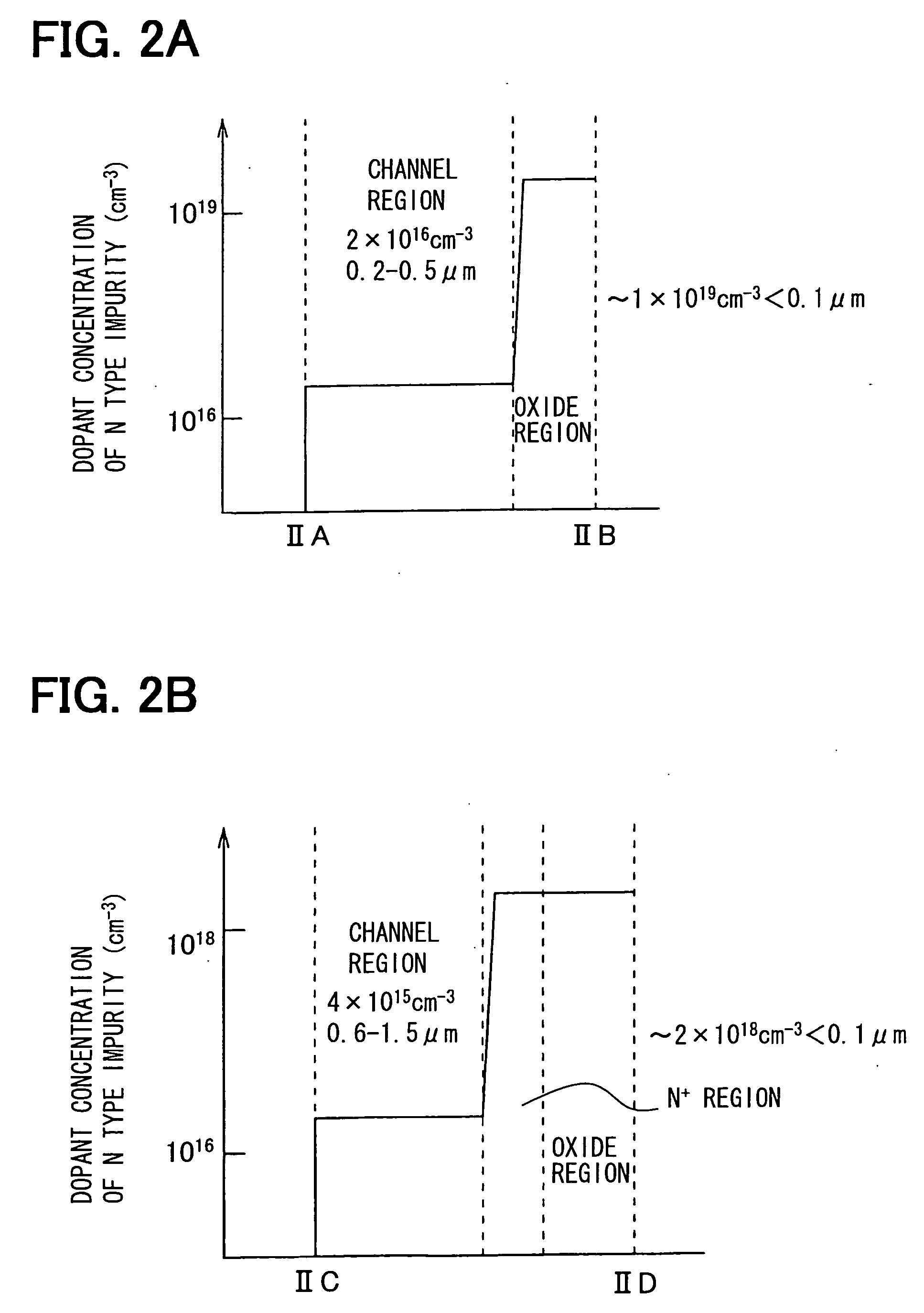
[0128]FIG. 31 shows profiles of the film thicknesses of the N− type channel layer 6 and the oxide film 8 and the dopant concentration of the N type impurities on line XXXIA-XXXIB within FIG. 30.
[0129] On line XXXI...
PUM
 Abstract
Description
Claims
Application Information
 - R&D
- Intellectual Property
- Life Sciences
- Materials
- Tech Scout
- Unparalleled Data Quality
- Higher Quality Content
- 60% Fewer Hallucinations
Browse by: Latest US Patents, China's latest patents, Technical Efficacy Thesaurus, Application Domain, Technology Topic, Popular Technical Reports.
© 2025 PatSnap. All rights reserved.Legal|Privacy policy|Modern Slavery Act Transparency Statement|Sitemap|About US| Contact US: help@patsnap.com