Integrated circuit memory devices having hierarchical bit line selection circuits therein

a technology of integrated circuit memory and hierarchical selection circuit, which is applied in the direction of digital storage, semiconductor devices, instruments, etc., can solve the problems of potent destructive regenerative current conduction within the substrate, and achieve the effects of reducing active power requirements, reducing bit line capacitance, and reducing layout area requirements

Inactive Publication Date: 2006-03-23
SAMSUNG ELECTRONICS CO LTD
View PDF8 Cites 33 Cited by
  • Summary
  • Abstract
  • Description
  • Claims
  • Application Information

AI Technical Summary

Benefits of technology

[0008] Integrated circuit memory devices according to embodiments of the invention utilize hierarchical bit line selection circuits to reduce active power requirements by lowering bit line capacitance. These memory devices also include arrangements of stacked thin-film transistors (TFTs), which reduce the layout area requirements of bit line precharge and selection circuits. According to some of these embodiments of the invention, a memory device includes at least a first column of memory cells electrically coupled to a first pair of bit lines. A bit line precharge and selection circuit is also provided. This bit line precharge and selection circuit includes a stacked arrangement of a first PMOS pull-up transistor and a first NMOS pass transistor electrically coupled to one of the first pair of bit lines. This stacked arrangement of transistors may be disposed above a memory core portion of a semiconductor substrate and thereby reduce the presence of alternating P-type and N-type conductivity regions within the memory core portion. This reduction in alternating P-type and N-type conductivity regions operates to inhibit an occurrence of parasitic latch-up, which may result in potentially destructive regenerative current conduction within the substrate.

Problems solved by technology

This reduction in alternating P-type and N-type conductivity regions operates to inhibit an occurrence of parasitic latch-up, which may result in potentially destructive regenerative current conduction within the substrate.

Method used


Image

  • Integrated circuit memory devices having hierarchical bit line selection circuits therein
  • Integrated circuit memory devices having hierarchical bit line selection circuits therein
  • Integrated circuit memory devices having hierarchical bit line selection circuits therein

Examples


Embodiment Construction

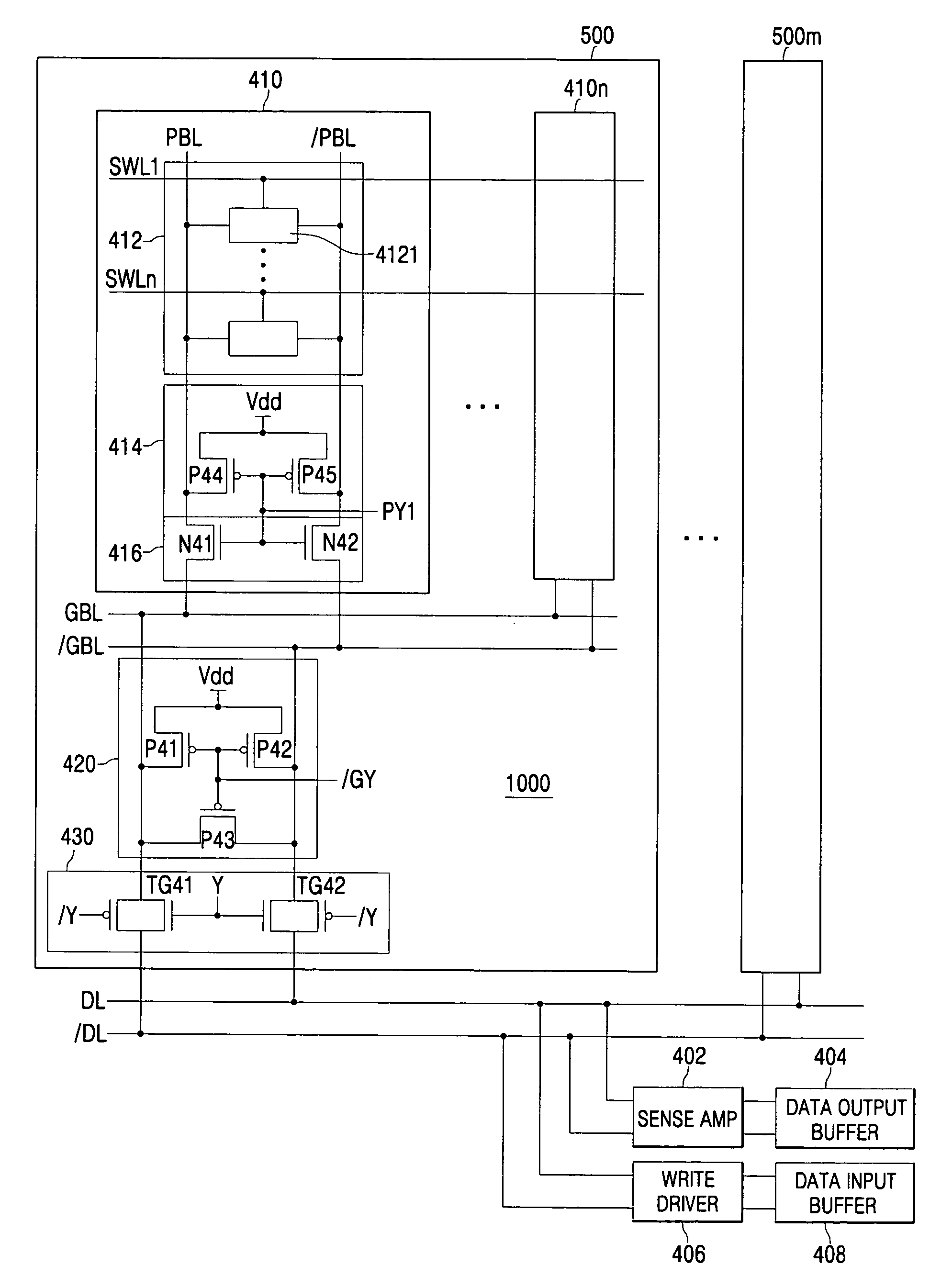
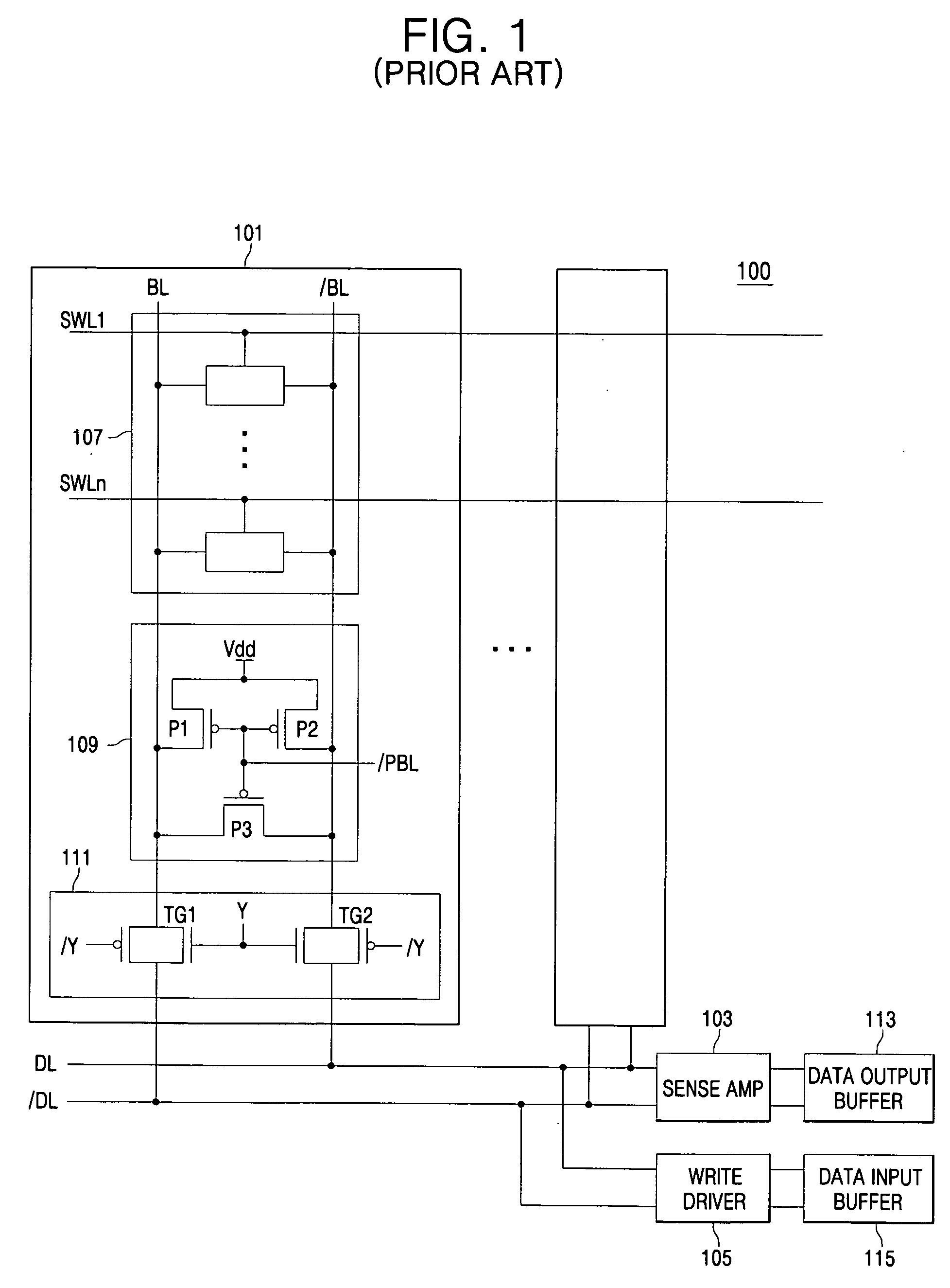
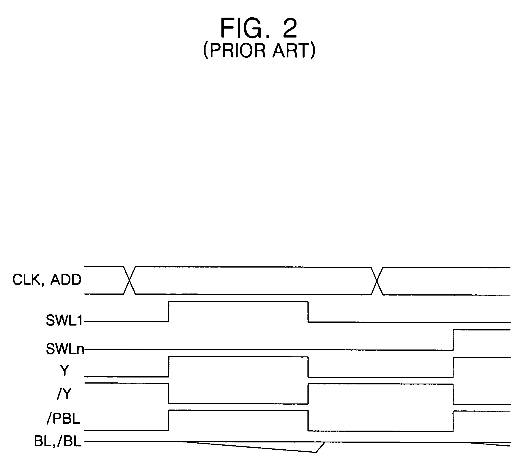
[0020] The present invention now will be described more fully herein with reference to the accompanying drawings, in which preferred embodiments of the invention are shown. This invention may, however, be embodied in many different forms and should not be construed as being limited to the embodiments set forth herein; rather, these embodiments are provided so that this disclosure will be thorough and complete, and will fully convey the scope of the invention to those skilled in the art. In the drawings, the thickness of layers and regions are exaggerated for clarity of description. It will also be understood that when a layer is referred to as being “on” another layer or substrate, it can be directly on the other layer or substrate, or intervening layers may also be present. Like reference numerals refer to like elements throughout. Signals may also be synchronized and / or undergo minor boolean operations (e.g., inversion) without being considered different signals. The suffix B (or ...


PUM


Abstract

Integrated circuit memory devices include a first column of memory cells electrically coupled to a first pair of bit lines and a bit line precharge and selection circuit. This bit line precharge and selection circuit includes at least one stacked arrangement of thin-film transistors. These thin-film transistors include a first PMOS thin-film pull-up transistor and a first NMOS thin-film pass transistor. These thin-film transistors are electrically coupled to one of the first pair of bit lines. The first column of memory cells includes a column of TFT SRAM cells.

Description

REFERENCE TO PRIORITY APPLICATION [0001] This application claims priority to Korean Application Serial No. 2004-75252, filed Sep. 20, 2004, the disclosure of which is hereby incorporated herein by reference. FIELD OF THE INVENTION [0002] The present invention relates to integrated circuit devices and methods of operating same and, more particularly, to integrated circuit memory devices and methods of operating same. BACKGROUND OF THE INVENTION [0003] Conventional memory devices include a class of memory devices referred to as static random access memory (SRAM) devices. As illustrated by FIG. 1, a conventional SRAM device 100 includes a plurality of column units 101 arranged side-by-side in a semiconductor substrate. Each of the column units 101 is illustrated as including a column of SRAM cells 107, a bit line precharging and equalization circuit 109, which is responsive to an active low bit line precharge signal / PBL, and a bit line selection circuit 111, which is responsive to a p...

Claims


Application Information

Patent Timeline
Patent Type & Authority Applications(United States)
IPC IPC(8): G11C7/00
CPCG11C7/12G11C7/18H01L27/1108H01L27/0688G11C2207/002H10B10/125
Inventor SUH, YOUNG-HOBYUN, HYUN-GEUN
Owner SAMSUNG ELECTRONICS CO LTD
Why Eureka
Try Eureka