Method for preparing a semiconductor memory structure

a memory structure and semiconductor technology, applied in semiconductor devices, digital storage, instruments, etc., can solve the problems of degrading the performance of the dram cell, the disturbance of the word line in adjacent word lines, and the size of the device, so as to increase the density of the device, reduce the disturbance of the word line, and reduce the capacitance of the word line to the word line.

Active Publication Date: 2019-06-27
NAN YA TECH
View PDF2 Cites 1 Cited by
  • Summary
  • Abstract
  • Description
  • Claims
  • Application Information

AI Technical Summary

Benefits of technology

[0026]In the present disclosure, a method for preparing the semiconductor memory structure is provided. Using the two etching processes, adjacent pairs of buried digit lines are spaced apart from each other by the isolation structures. By forming the buried word lines having the bottom surfaces higher than the top surfaces of the buried digit lines, adjacent pairs of buried word lines are spaced apart from each other by the isolation structures over the buried digit lines. Consequently, both word line to word line capacitance and digit line to digit line capacitance are reduced. Further, a semiconductor memory structure including a plurality of buried word lines and a plurality of buried digit lines are provided. Since both of the word lines and digit lines are buried in the substrate, the semiconductor memory structure provides vertical structures, which help to increase device density. Further, the buried word lines and the buried digit lines are alternately arranged. Since pairs of buried word lines are spaced apart from each other by the isolation structures, channel regions are also spaced apart from each other by those isolation structures, and thus word line disturbance is further reduced.

Problems solved by technology

However, as the reduction of the device size also reduces the distance between the word lines and the bit lines, word line disturbance is observed in adjacent word lines.
When the word line disturbance becomes serious, performance of the DRAM cell is degraded.
In contrast, with a comparative DRAM memory structure, pairs of word lines that share one digit line also share the same channel region, and thus always suffer from word line disturbance.

Method used


Image

  • Method for preparing a semiconductor memory structure
  • Method for preparing a semiconductor memory structure
  • Method for preparing a semiconductor memory structure

Examples


Embodiment Construction

[0036]Embodiments, or examples, of the disclosure illustrated in the drawings are now described using specific language. It shall be understood that no limitation of the scope of the disclosure is hereby intended. Any alteration or modification of the described embodiments, and any further applications of principles described in this document, are to be considered as normally occurring to one of ordinary skill in the art to which the disclosure relates. Reference numerals may be repeated throughout the embodiments, but this does not necessarily mean that feature(s) of one embodiment apply to another embodiment, even if they share the same reference numeral.

[0037]It shall be understood that, although the terms first, second, third, etc. may be used herein to describe various elements, components, regions, layers or sections, these elements, components, regions, layers or sections are not limited by these terms. Rather, these terms are merely used to distinguish one element, component...


PUM


Abstract

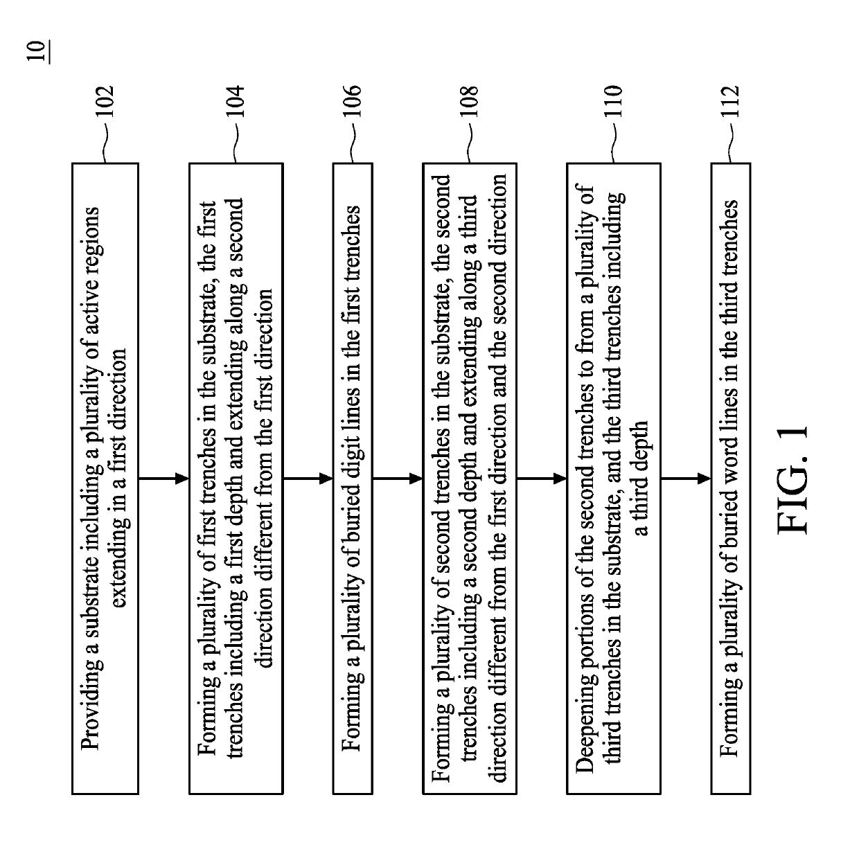
The present disclosure provides a method for preparing a semiconductor memory structure. The method includes the following steps: providing a substrate comprising a plurality of active regions extending in a first direction; forming a plurality of first trenches in the substrate, the first trenches comprising a first depth and extending in a second direction different from the first direction; forming a plurality of buried digit lines in the first trenches; forming a plurality of second trenches in the substrate, the second trenches comprising a second depth and extending in a third direction different from the first direction and the second direction; deepening portions of the second trenches to form a plurality of third trenches in the substrate, the third trenches comprising a third depth; and forming a plurality of buried word lines in the third trenches.

Description

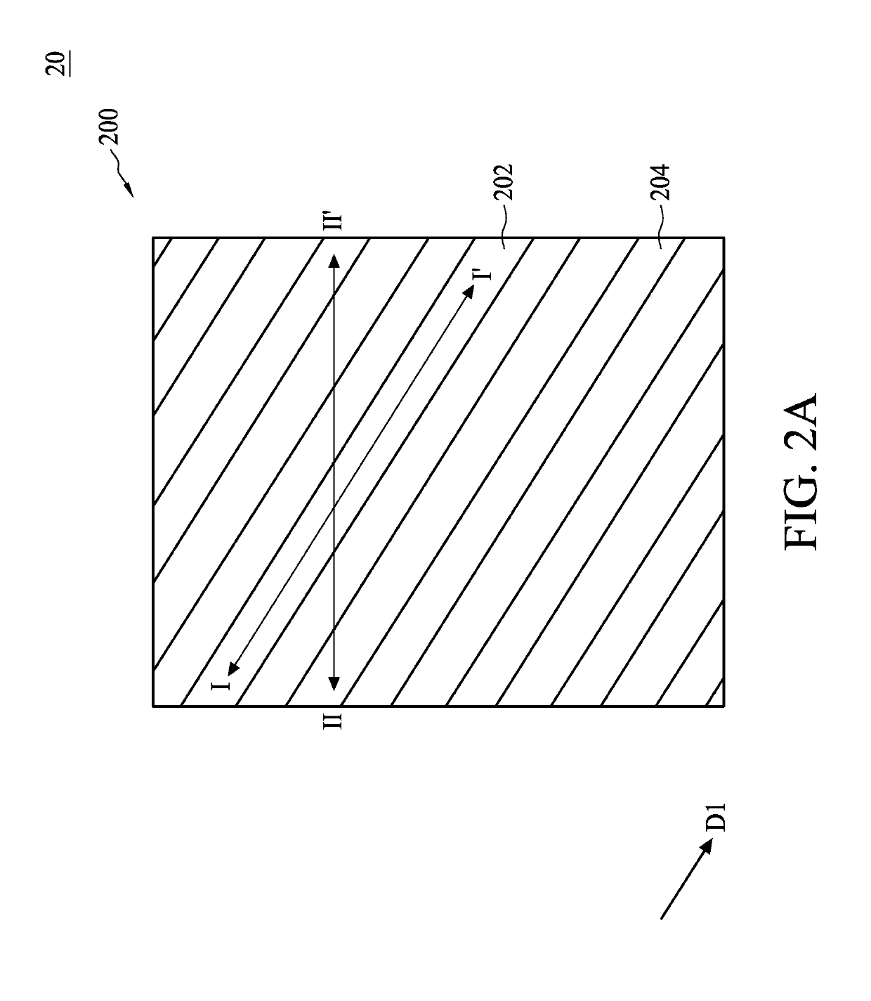
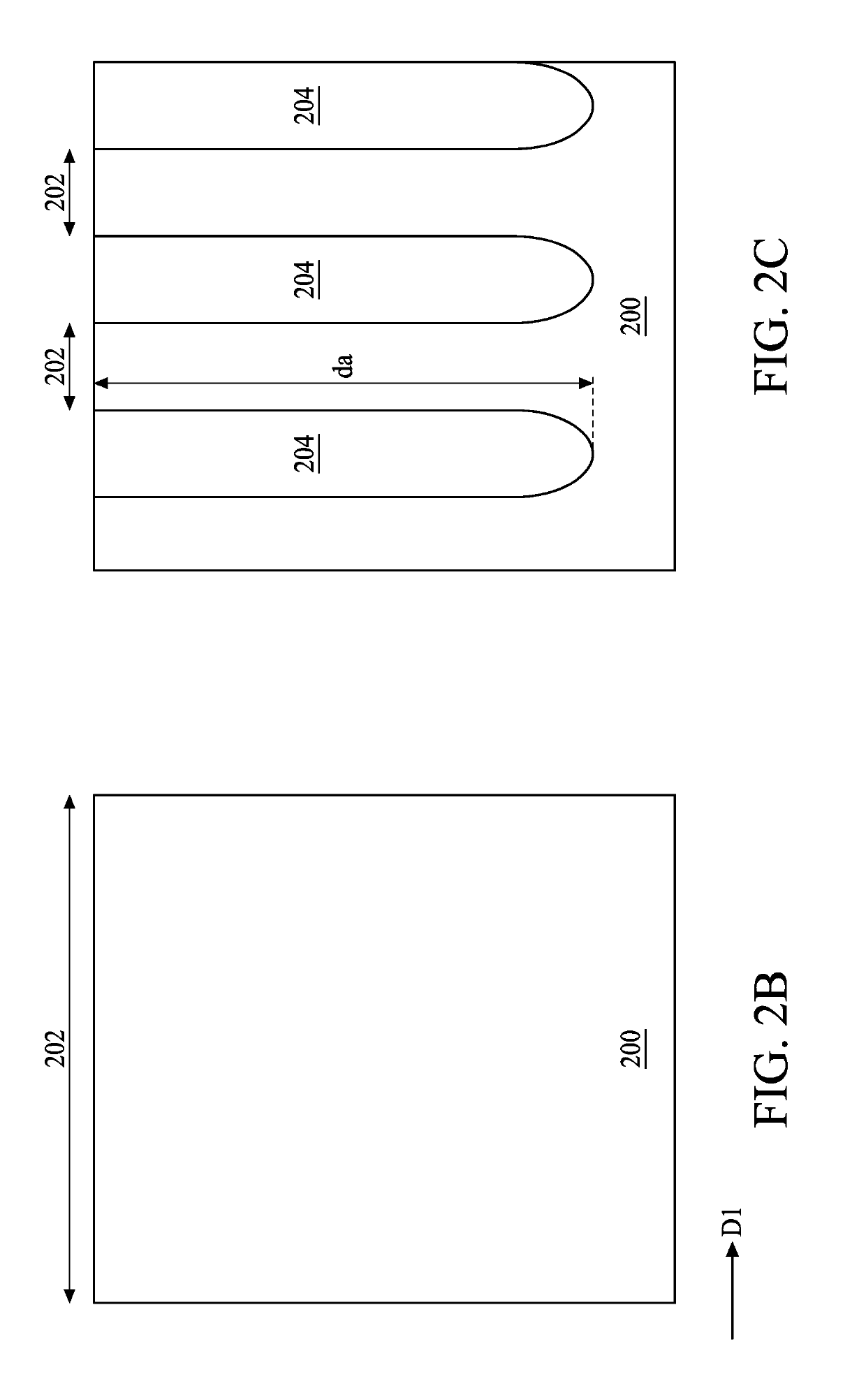
PRIORITY CLAIM AND CROSS-REFERENCE[0001]This application is a divisional application of U.S. application Ser. No. 15 / 867,043, filed on Jan. 10, 2018, which claims the benefit of U.S. Provisional Patent Application Ser. No. 62 / 610,264 filed on Dec. 25, 2017. The entireties of the above-mentioned patent applications are hereby incorporated by reference herein and made a part of this specification.TECHNICAL FIELD[0002]The present disclosure relates to a semiconductor memory structure and a method for preparing the same, and more particularly, to a semiconductor dynamic random access memory (DRAM) structure and a method for preparing the same.DISCUSSION OF THE BACKGROUND[0003]Electrical products are becoming lighter, thinner, shorter, and smaller, and DRAMs are being scaled down to match the trends of high integration and high density. A DRAM including many memory cells is one of the most popular volatile memory devices utilized today. Each memory cell includes a transistor and at least...

Claims


Application Information

Patent Timeline
Patent Type & Authority Applications(United States)
IPC IPC(8): H01L27/108G11C11/401
CPCH01L27/10882H01L27/10838G11C11/401H01L27/1087H10B43/30H10B12/34H10B12/053H10B12/488H10B12/0335H10B12/482H10B12/39H10B12/48H10B12/0387
Inventor LIAO, WEI-MING
Owner NAN YA TECH
Why Eureka
Try Eureka