Reduction of a feature dimension in a nano-scale device

a nano-scale device and feature dimension technology, applied in the field of nano-scale devices, can solve the problems of ineffective improvement, serial repetition of steps in e-beam and x-ray lithographic processes, and low cost effectiveness, and achieve the effect of reducing the core width of the first nanowire and reducing the feature dimension

Inactive Publication Date: 2006-03-23
HEWLETT PACKARD DEV CO LP
View PDF16 Cites 26 Cited by
  • Summary
  • Abstract
  • Description
  • Claims
  • Application Information

AI Technical Summary

Benefits of technology

[0010] In other embodiments of the present invention, a nano-scale device with reduced feature dimensions is provided. The nano-scale device comprises first nanowires formed on a substrate. The first nanowires are spaced apart on the substrate. The nano-scale device further comprises a second nanowire added on the substrate in a gap between adjacent ones of the first nanowires. The second nanowire and the first nanowires have a similar material characteristic. The added second nanowire effectively decreases a core width of the first nanowires.

Problems solved by technology

In addition, the e-beam and x-ray lithographic processes are very slow processes rendering such serial repetition of steps undesirable for achieving smaller dimensions.
Such improvements are not cost effective since an inherent limitation in these lithographic processes restricts achieving features sizes smaller than about 15 nm.

Method used


Image

  • Reduction of a feature dimension in a nano-scale device
  • Reduction of a feature dimension in a nano-scale device
  • Reduction of a feature dimension in a nano-scale device

Examples


Embodiment Construction

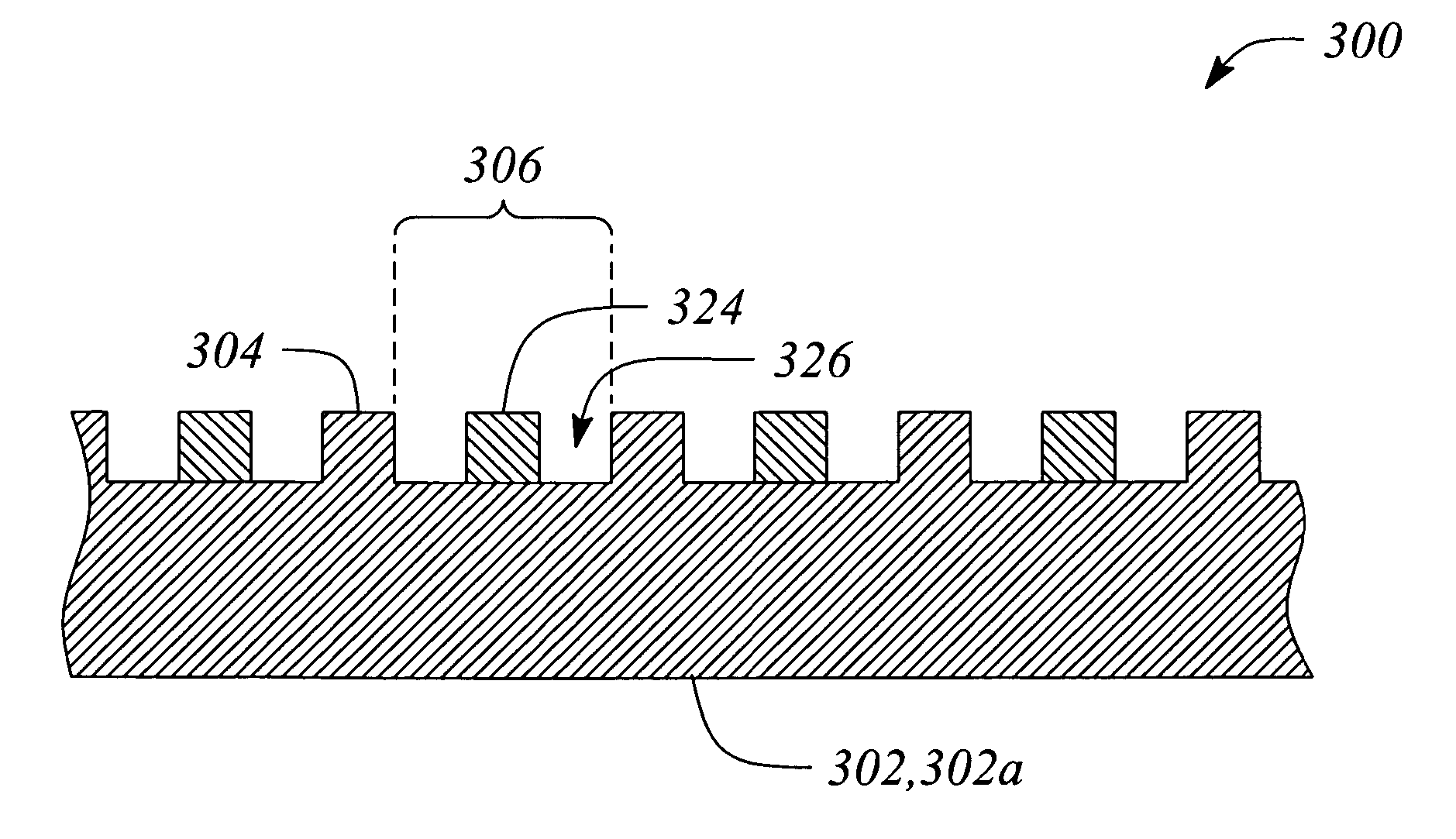
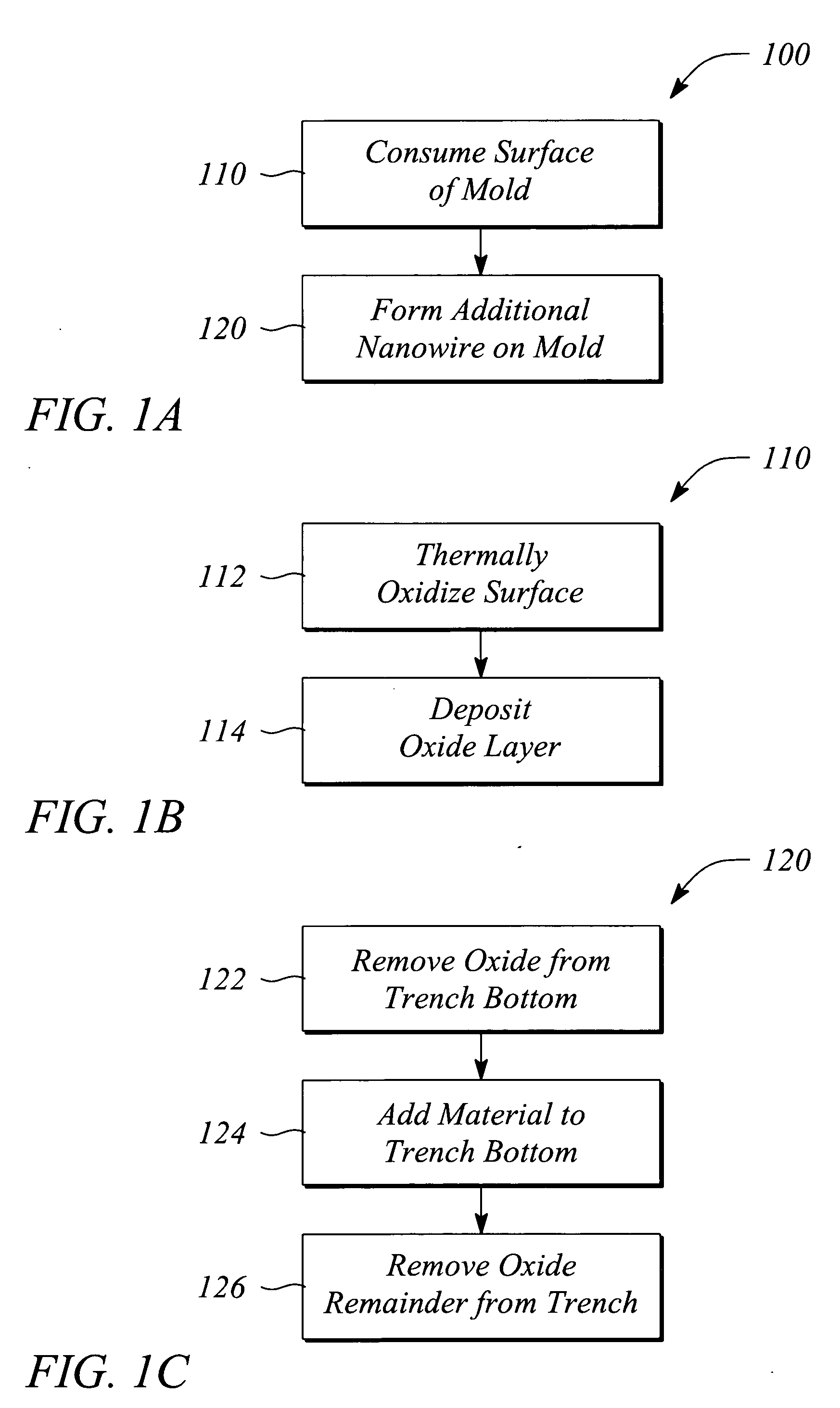
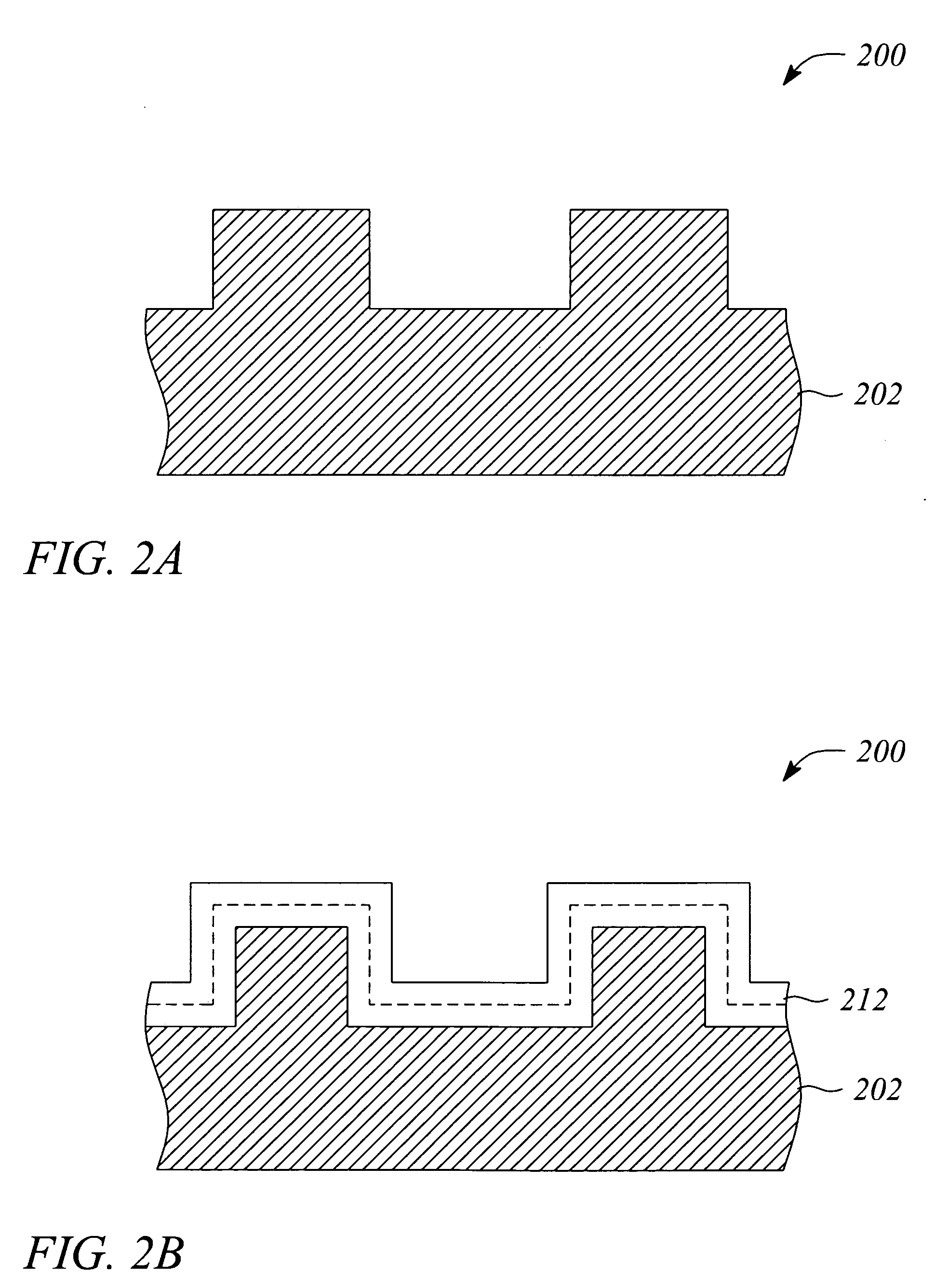
[0019] Embodiments of the present invention are directed to fabrication of nano-scale devices or structures and nano-scale devices thus fabricated. In some embodiments, the device fabrication and the device thus fabricated are used in imprint lithography. In some embodiments, the device fabrication and the device thus fabricated are used in one or more of photonic, electronic, sensing, nanofluidic and catalysis applications, for example. In each embodiment, the fabrication and the fabricated device includes consumption of a substrate surface to form a sacrificial sheath or shell on the substrate that is later removed. When the sheath is removed, a core dimension of the substrate is reduced that translates to a reduced dimension of a feature defined on the substrate surface. As such, smaller and / or closer spaced nano-scale features can be achieved on the substrate than features achieved without the consumption. In particular, one or more of size, spacing and / or pitch of the features ...


PUM

PropertyMeasurementUnit
widthaaaaaaaaaa
widthaaaaaaaaaa
feature widthaaaaaaaaaa

Abstract

Nano-scale devices and methods provide reduced feature dimensions of features on the devices. A surface of a device substrate having a pattern of spaced apart first nanowires is consumed, such that a dimension of the first nanowires is reduced. A second nanowire is formed in a trench or gap between adjacent ones of the first nanowires, such that the nano-scale device includes a set of features that includes the first nanowires with the reduced dimension and the second nanowire spaced from the adjacent first nanowires by sub-trenches.

Description

STATEMENT REGARDING FEDERALLY SPONSORED RESEARCH OR DEVELOPMENT [0001] The U.S. Government has a paid-up license in this invention and the right in limited circumstances to require the patent owner to license others on reasonable terms as provided for by the terms of Contract No. MDA972-01-3-0005 awarded by the Defense Advanced Research Projects Agency.BACKGROUND [0002] 1. Technical Field [0003] The invention relates to nano-scale devices and the fabrication of nano-scale devices. In particular, the invention relates to reducing a size, spacing and / or pitch dimension of features in a nano-scale device or structure. [0004] 2. Description of Related Art [0005] A consistent trend in semiconductor technology since its inception is toward smaller and smaller device dimensions and higher and higher device densities. As a result, an area of semiconductor technology that recently has seen explosive growth and generated considerable interest is nanotechnology. Nanotechnology is concerned wit...

Claims


Application Information

Patent Timeline
Patent Type & Authority Applications(United States)
IPC IPC(8): H01L21/4763
CPCB81C99/009B81C2201/0153G03F7/0002B82Y40/00B82Y10/00Y10T428/31612
Inventor SHARMA, SHASHANK
Owner HEWLETT PACKARD DEV CO LP
Why Eureka
Try Eureka