Active matrix light emitting device display pixel circuit and drive method

a technology of active matrix and light emitting device, applied in the direction of instruments, computing, electric digital data processing, etc., can solve the problems of reducing device variation across, increasing the complexity of pixel circuit, and affecting the effect of threshold voltage variation

Inactive Publication Date: 2006-03-30
CHOU CHEN JEAN
View PDF16 Cites 70 Cited by
  • Summary
  • Abstract
  • Description
  • Claims
  • Application Information

AI Technical Summary

Benefits of technology

[0022] Preferred embodiments of the present invention are provided for the operation of a display in current drive scheme to eliminate dependency on threshold voltage variation and OLED characteristics. Preferred embodiments in three-transistor implementation are provided to illustrate the application to the solutions for current drive scheme for light emitting device display. Furthermore, current drive scheme is demonstrated in common cathode, n-channel transistor drive configuration.

Problems solved by technology

The major challenges in achieving such a commercialization include (1) improving the material and device operating life, and (2) reducing device variation across the display area.
As more elaborated control circuits being incorporated into individual pixels as proposed in these solutions, concerns over complexity and practical manufacturing issues arise.
Comparing to the basic pixel circuit in FIG. 2, it is evident that any current solution to the uniformity issue involves a substantial increase in the complexity of pixel circuit, and thus likelihood of reduction of available light emitting area, efficiency, and product yield.

Method used


Image

  • Active matrix light emitting device display pixel circuit and drive method
  • Active matrix light emitting device display pixel circuit and drive method
  • Active matrix light emitting device display pixel circuit and drive method

Examples


Embodiment Construction

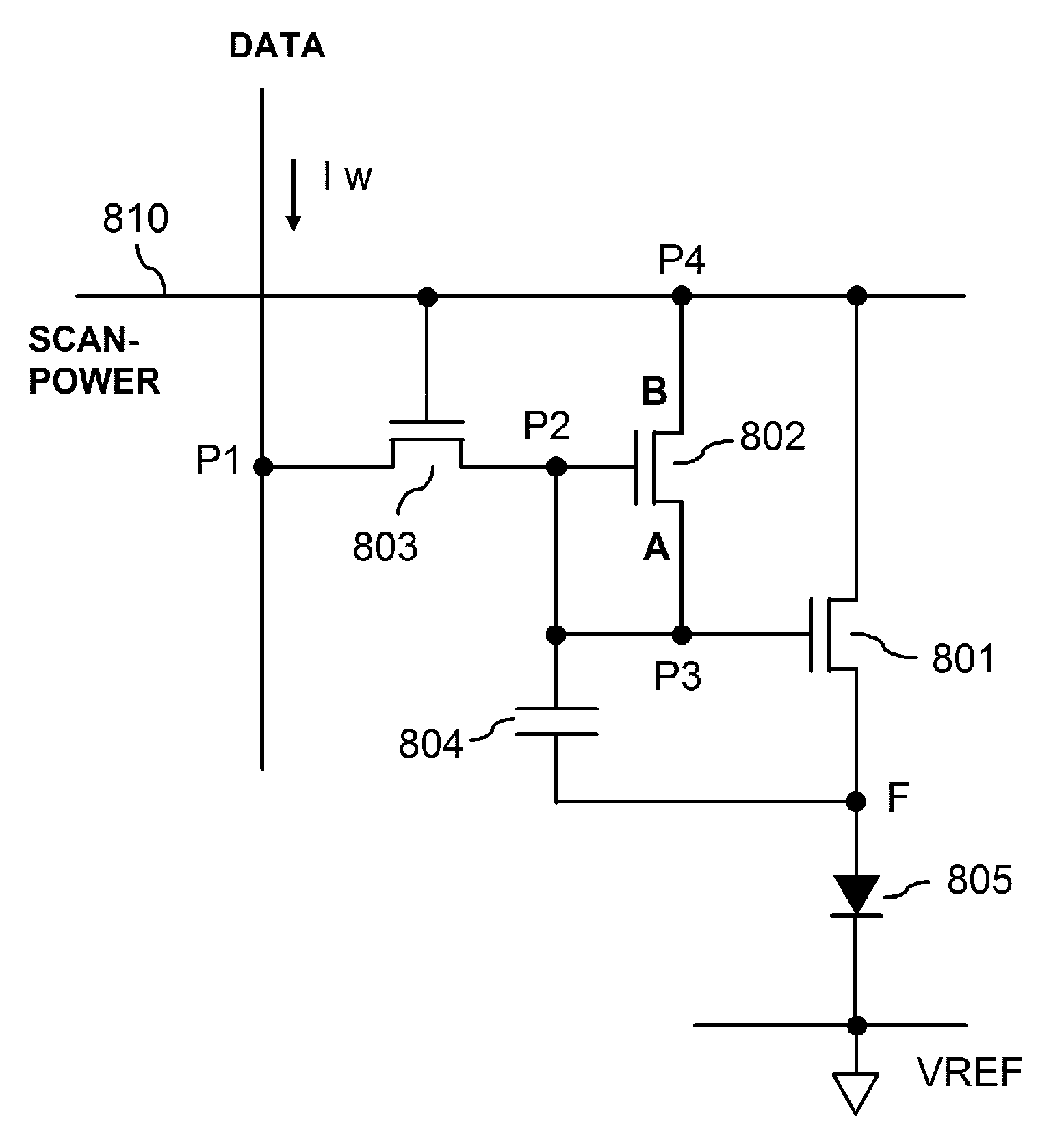
[0042] The present invention is directed to the operation of active matrix displays. Preferred embodiments and respective claims are described in light of the application to light emitting device display.

[0043] Preferred embodiments of the present invention are herein described using organic light emitting diodes as illustration. Examples of using organic material to form an LED are found in U.S. Pat. No. 5,482,896 and U.S. Pat. No. 5,408,109, and examples of using organic light emitting diode to form active matrix display devices are found in U.S. Pat. No. 5,684,365 and U.S. Pat. No. 6,157,356, all of which are hereby incorporated by reference.

[0044] Herein in this specification, voltages and potentials in an embodiment are referenced to a reference voltage level VREF in that embodiment. The meaning of voltage and potential are thus interchangeable within each respective case. Claimed subjects follow the same descriptive convention.

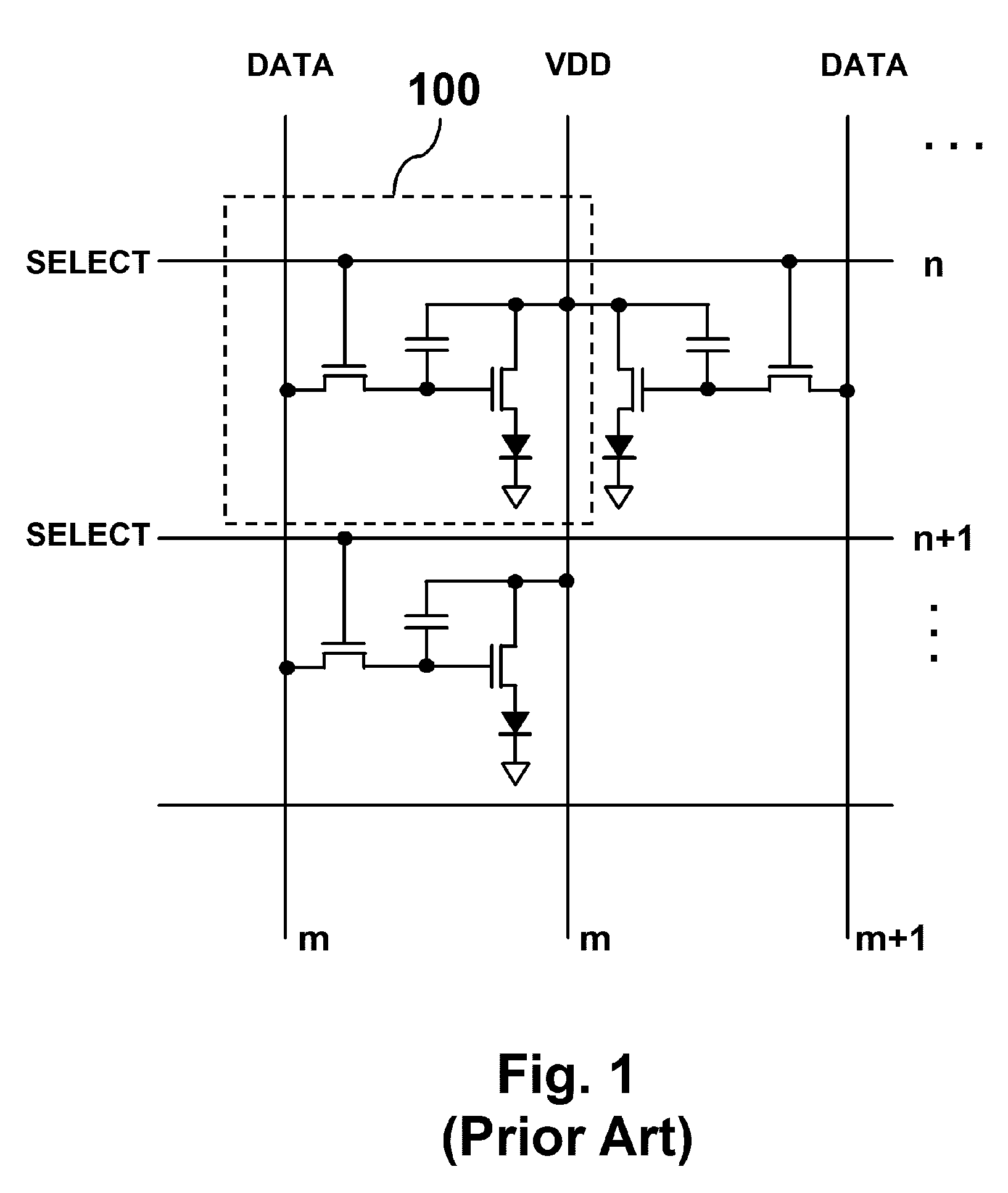
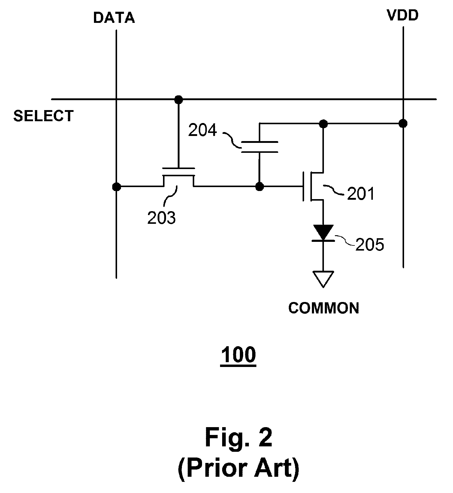
[0045] As evidenced in the prior art illustrate...


PUM


Abstract

Display pixel circuits and a drive scheme utilizing a switching element operating in reverse direction in a data scan period to provide voltage reference are provided. Preferred embodiments and operation method leading to three-transistor solutions in current-control mode, common-cathode, and n-channel transistor drive configuration for light emitting device display are described.

Description

CROSS REFERENCE [0001] The present application is claiming the priority of U.S. Provisional Patent Application No. 60 / 522,396, filed on Sep. 24, 2004.BACKGROUND OF THE INVENTION [0002] 1. Field of the Invention [0003] The present invention relates to the pixel circuit of active matrix displays and a drive scheme to operate the displays comprising such pixel circuits. Pixel circuits and a method are provided to set a data in a pixel and to deliver a drive current to the pixel according to said data setting. [0004] Furthermore, the present invention relates to the pixel circuits and drive method of an active matrix display, where the pixel circuits comprise active elements, such as thin film transistors, for controlling the light emitting operation of the respective light emitting devices in a pixel. More specifically, the present invention provides structures of pixel circuit that combines a data setting circuit formed between a data electrode and a scan electrode, and a voltage refe...

Claims


Application Information

Patent Timeline
Patent Type & Authority Applications(United States)
IPC IPC(8): G09G3/30
CPCG09G3/3241G09G2300/0417G09G2300/0809G09G2300/0842G09G2320/043G09G2300/0866G09G2310/0251G09G2310/0256G09G2320/0233G09G2300/0847
Inventor CHOU, CHEN-JEAN
Owner CHOU CHEN JEAN
Why Eureka
Try Eureka