High-brightness gallium-nitride based light emitting diode structure

Inactive Publication Date: 2006-04-27
FORMOSA EPITAXY INCORPORATION +1
View PDF9 Cites 19 Cited by
  • Summary
  • Abstract
  • Description
  • Claims
  • Application Information

AI Technical Summary

Benefits of technology

[0007] Therefore, the present invention provides an epitaxial structure for the GaN-based LE

Problems solved by technology

As such, total internal reflection would occur and photons released from the active layer would

Method used


Image

  • High-brightness gallium-nitride based light emitting diode structure
  • High-brightness gallium-nitride based light emitting diode structure
  • High-brightness gallium-nitride based light emitting diode structure

Examples


first embodiment

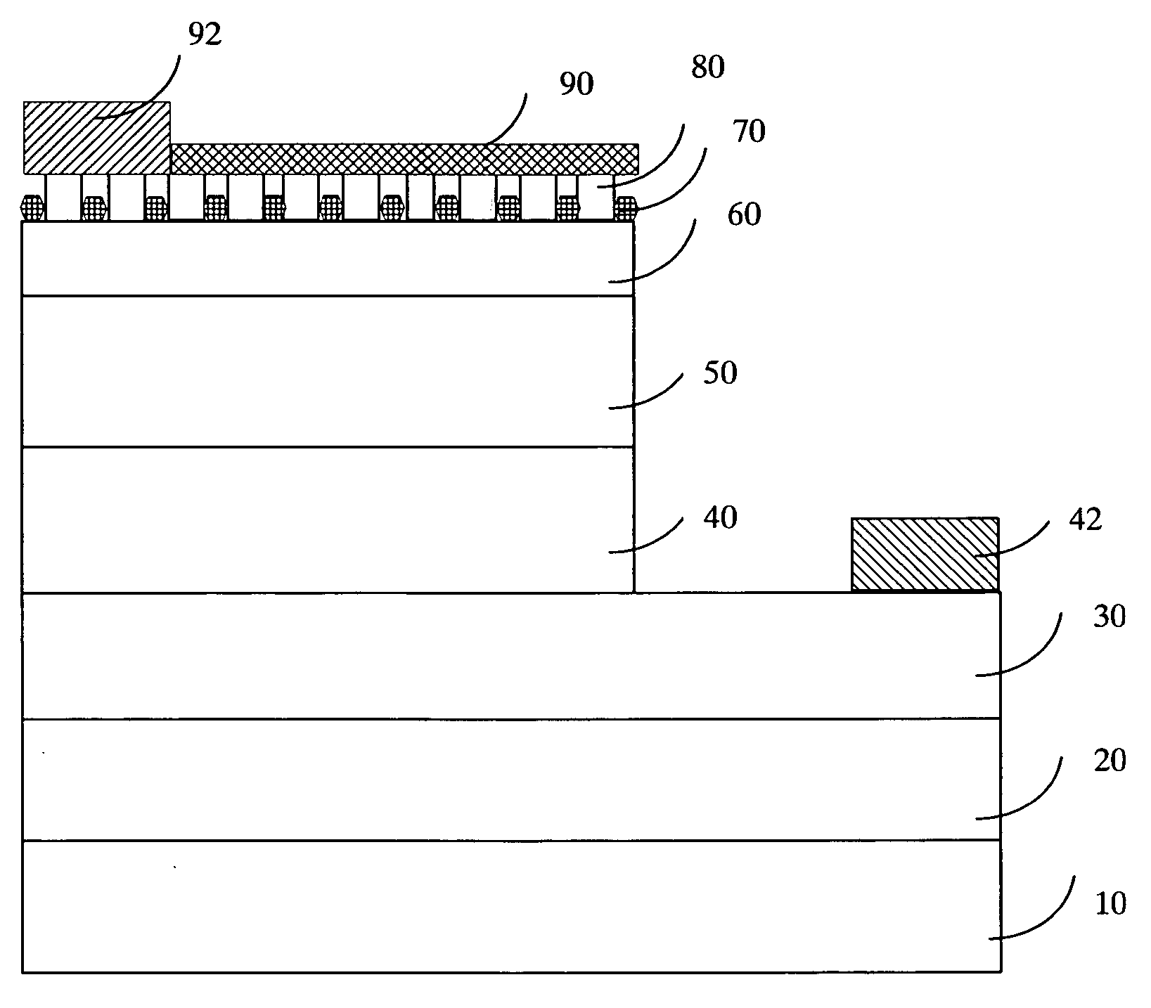
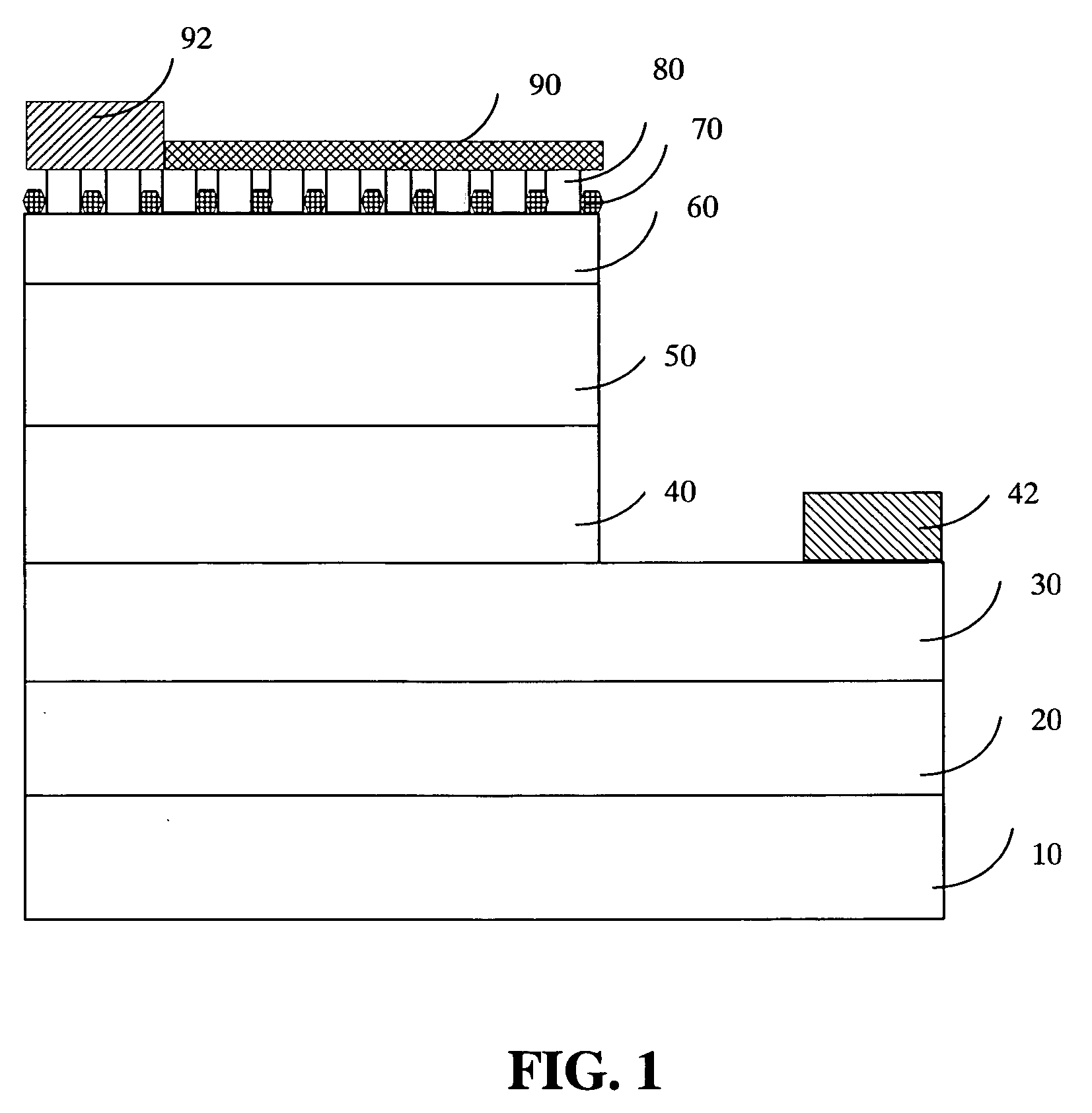
[0016]FIG. 1 is a schematic diagram showing the epitaxial structure of the GaN-based LEDs according to the present invention. As shown in FIG. 1, the GaN-based LED has a substrate 10 made of C-plane, R-plane, or A-plane aluminum-oxide monocrystalline (sapphire), or an oxide monocrystalline having a lattice constant compatible with that of nitride semiconductors. The substrate 10 can also be made of SiC (6H—SiC or 4H—SiC), Si, ZnO, GaAs, or MgAl2O4. Generally, the most common material used for the substrate 10 is sapphire or SiC. A buffer layer 20 made of AlaGabIn1-a-bN (0≦a,b10. Then, an n-type contact layer 30 made of a GaN-based material is formed on the buffer layer 20. On top of the n-type contact layer 30, there are an active layer 40 made of indium-gallium-nitride (InGaN) and a negative electrode 42, not overlapping with each other.

[0017] The present embodiment then forms a p-type cladding layer 50 made of a p-type GaN-based material on top of the active layer 40. In turn, on ...

second embodiment

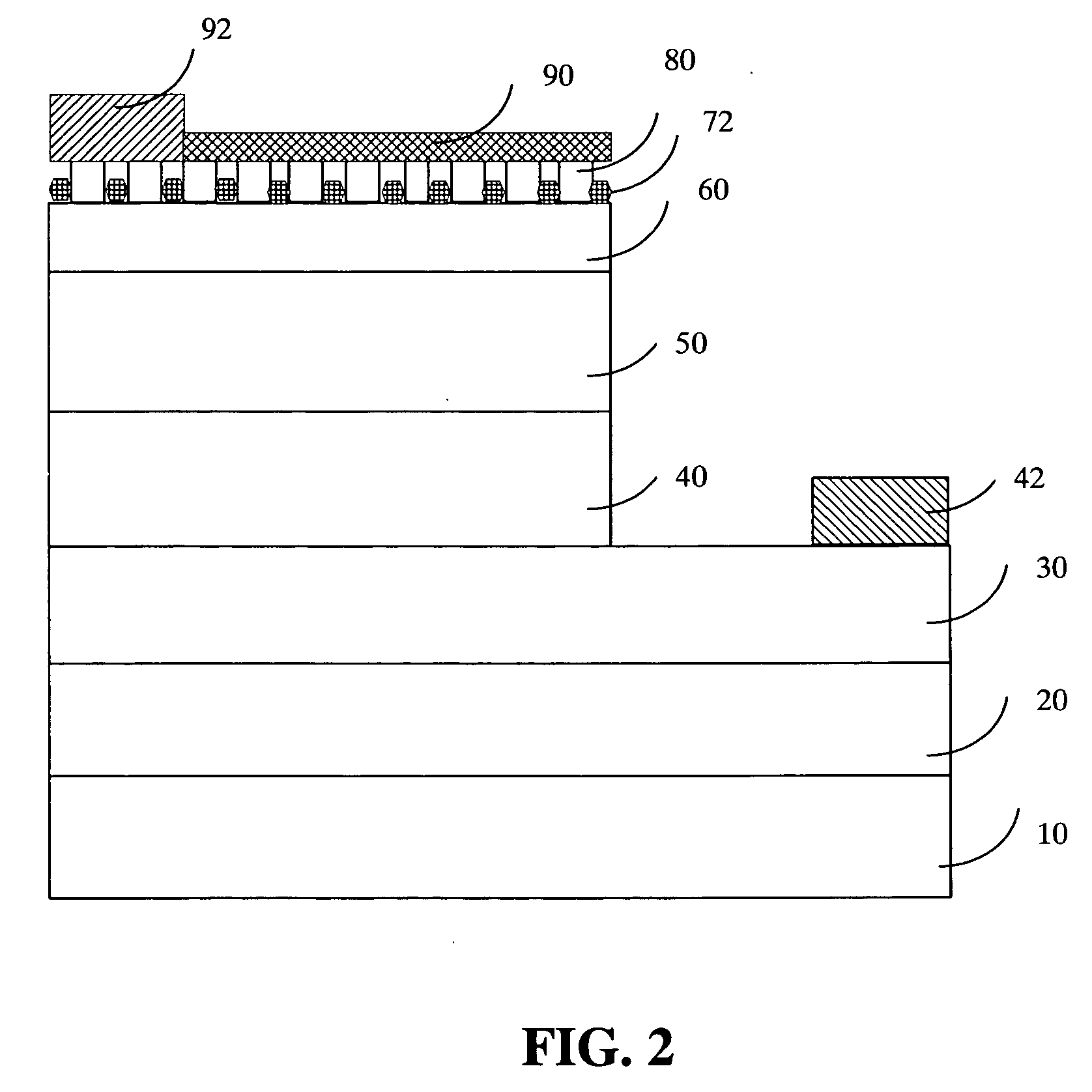
[0020]FIG. 2 is a schematic diagram showing the epitaxial structure of the GaN-based LEDs according to the present invention. As shown in FIG. 2, the present embodiment has an identical structure as in the previous embodiment. The only difference lies in the material used for the masking buffer layer. Within the present embodiment, the masking buffer layer 72 is developed also by MOCVD using MggNh (g,h≧1) having a specific composition up to a thickness between 5 Å and 100 Å under a growing temperature between 600° C. and 1100° C. The masking buffer layer 72 is also a mask containing multiple randomly distributed MggNh clusters.

[0021] The present embodiment then develops a p-type roughened contact layer 80 made of AliInjGa1-i-jN, (0≦i,j80 does not grow directly on top of the masking buffer layer 72. Instead, the p-type roughened contact layer 80 starts from the top surface of the underlying p-type contact layer 60 not covered by the masking buffer layer 72's MggNh clusters. The p-typ...

third embodiment

[0022]FIG. 3 is a schematic diagram showing the epitaxial structure of the GaN-based LEDs according to the present invention. As shown in FIG. 3, the present embodiment has an identical structure as in the previous embodiment. The only difference lies in the material used for the masking buffer layer. Within the present embodiment, the masking buffer layer 74 is developed also by MOCVD using heavily doped (>1×1020 cm−3) AlkInlGa1-k-lN (0≦k,l72 is also a mask containing multiple randomly distributed AlkInlGa1-k-lN clusters.

[0023] The present embodiment then develops a p-type roughened contact layer 80 made of AlmInnGa1-m-nN, (0≦m,n80 does not grow directly on top of the masking buffer layer 74. Instead, the p-type roughened contact layer 80 starts from the top surface of the underlying p-type contact layer 60 not covered by the masking buffer layer 74's AlkInlGa1-k-lN clusters. The p-type roughened contact layer 80 then grows upward until it passes (but does not cover) the mask of th...


PUM


Abstract

A GaN-based LED structure is provided so that the brightness and luminous efficiency of the GaN-based LED are enhanced effectively. The greatest difference between the GaN-based LEDs according to the invention and the prior arts lies in the addition of a masking buffer layer on top of the p-type contact layer and a p-type roughened contact layer on top of the masking buffer layer. The masking buffer layer could be formed using MOCVD to deposit SixNy (x,y≧1), MgwNz (w,z≧1), or AlsIntGa1-s-tN (0≦s,t<1, s+t≦1) heavily doped with Si and/or Mg. The masking buffer layer is actually a mask containing multiple randomly distributed clusters. Then, on top of the masking buffer layer, a p-type roughened contact layer made of p-type AluInvGa1-u-vN (0≦u,v<1, u+v≦1) is developed. The p-type roughened contact layer does not grow directly on top of the masking buffer layer. Instead, the p-type roughened contact layer starts from the top surface of the underlying p-type contact layer not covered by the masking buffer layer's clusters. The p-type roughened contact layer then grows upward until it passes (but does not cover) the mask of the masking buffer layer for a specific distance. The total internal reflection that could have been resulted from the GaN-based LEDs' higher index of refraction than that of the atmosphere could be avoided. The GaN-based LEDs according to the present invention therefore have superior external quantum efficiency and luminous efficiency.

Description

BACKGROUND OF THE INVENTION [0001] 1. Field of the Invention [0002] The present invention generally relates to gallium-nitride based light emitting diodes and, more particularly, to the high-brightness gallium-nitride based light emitting diodes having roughened surfaces. [0003] 2. The Prior Arts [0004] Gallium-nitride (GaN) based light-emitting diodes (LEDs), as various colored LEDs can be developed by controlling the GaN-based material's composition, has been the research and development focus in the academic arena and in the industries as well in recent years. One of the research directions regarding GaN-based LEDs lies in the further understanding of the luminous characteristics of GaN-based LEDs. Based on this knowledge, then, methods for enhancing GaN-based LEDs' luminous efficiency and brightness can be developed and discovered. These high-efficiency and high-brightness GaN-based LEDs would soon find their widespread application in outdoor display panels and automobile lamps....

Claims


Application Information

Patent Timeline
IPC IPC(8): H01L33/00H01L33/14H01L33/22H01L33/32H01L33/42
CPCH01L33/14H01L33/22H01L33/32H01L33/42
Inventor WU, LIANG-WENTU, RU-CHINYU, CHENG-TSANGWEN, TZU-CHICHIEN, FEN-REN
Owner FORMOSA EPITAXY INCORPORATION
Why Eureka
Try Eureka