High-brightness gallium-nitride based light emitting diode structure

a light-emitting diode, high-bright technology, applied in the direction of basic electric elements, electrical equipment, semiconductor devices, etc., can solve the problem of reducing the external quantum efficiency

Inactive Publication Date: 2006-07-06
FORMOSA EPITAXY INCORPORATION +1
View PDF2 Cites 7 Cited by
  • Summary
  • Abstract
  • Description
  • Claims
  • Application Information

AI Technical Summary

Benefits of technology

[0008] Therefore, the present invention provides an epitaxial structure for the GaN-based LEDs so that the limitations and dis

Problems solved by technology

As such, total internal reflection would occur and photons released from the active layer would

Method used


Image

  • High-brightness gallium-nitride based light emitting diode structure
  • High-brightness gallium-nitride based light emitting diode structure
  • High-brightness gallium-nitride based light emitting diode structure

Examples


first embodiment

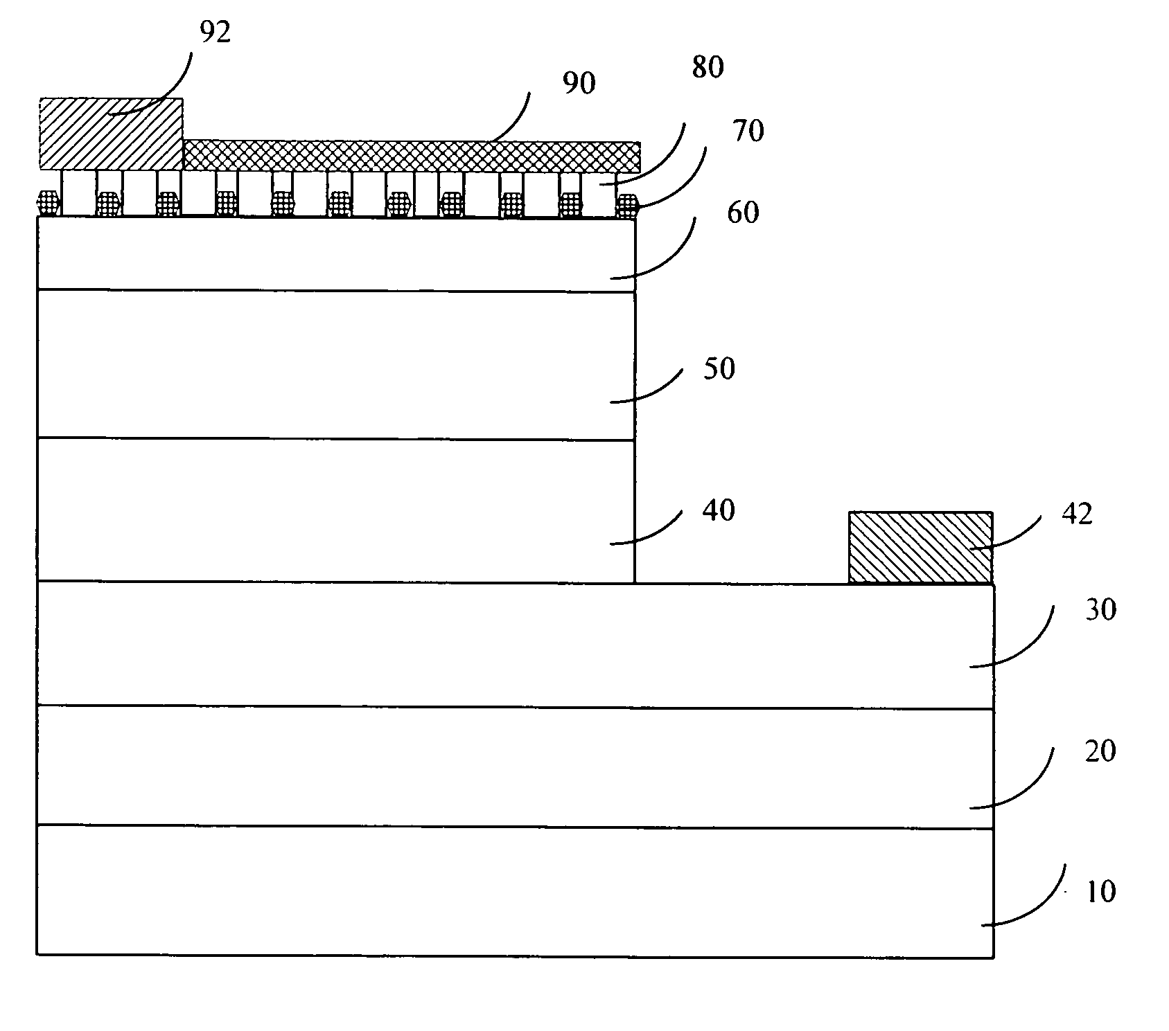
[0017]FIG. 1 is a schematic diagram showing a high-brightness GaN-based LED device according to the present invention. As shown in FIG. 1, the GaN-based LED device has a substrate 10 made of C-plane, R-plane, or A-plane aluminum-oxide monocrystalline (sapphire), or an oxide monocrystalline having a lattice constant compatible with that of nitride semiconductors. The substrate 10 can also be made of SiC (6H—SiC or 4H—SiC), Si, ZnO, GaAs, or MgAl2O4. Generally, the most common material used for the substrate 10 is sapphire or SiC. An optional buffer layer 20 made of a GaN-based material whose molecular formula could be expressed as AlaGabIn1-a-bN (0≦a,b10. On top of the buffer layer 20, a first contact layer 30 is formed and made of a GaN-based material having a first conduction type (e.g., it could be a p-typed GaN or n-typed GaN). Then, on top of the first contact layer 30, an active layer 40 made of a GaN-based material such as indium-gallium-nitride (InGaN) is formed on top of the...

second embodiment

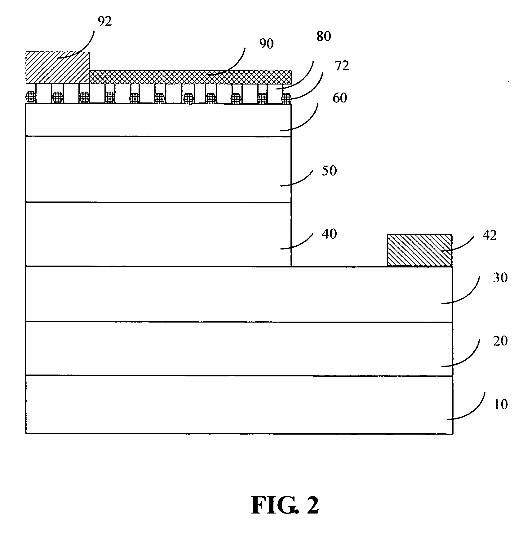
[0022]FIG. 2 is a schematic diagram showing a high-brightness GaN-based LED device according to the present invention. As shown in FIG. 2, the present embodiment has an identical structure as in the previous embodiment. The only difference lies in the material used for the masking buffer layer. In the present embodiment, the masking buffer layer 72 is developed also by a MOCVD process using a group-II nitride MggNh (g,h≧1) having a specific composition. The masking buffer layer 72 has a thickness between 5 Å and 100 Å and is formed at a growing temperature between 600° C. and 1100° C. Similarly, the masking buffer layer 72 thus formed contains multiple randomly distributed clusters of MggNh on top of the second contact layer 60.

third embodiment

[0023]FIG. 3 is a schematic diagram showing a high-brightness GaN-based LED device according to the present invention. As shown in FIG. 3, the present embodiment has an identical structure as in the previous embodiments. The only difference lies in the material used for the masking buffer layer. In the present embodiment, the masking buffer layer 74 is developed also by a MOCVD process using a heavily doped group-III nitride AlkInlGa1-k-lN (0≦k,lkInlGa1-k-lN is doped with at least a dopant selected from the group-II and group-IV elements. For example, the dopant used could be Si, Mg, or both Si and Mg could be used. The doping density is at least 1×1020 cm−3. The masking buffer layer 74 has a thickness between 5 Å and 100 Å and is formed at a growing temperature between 600° C. and 1100° C. Similarly, the masking buffer layer 74 thus formed contains multiple randomly distributed clusters of AlkInlGa1-k-lN on top of the second contact layer 60.

[0024] In aforementioned preferred embod...


PUM


Abstract

A GaN-based LED structure is provided so that the brightness and luminous efficiency of the GaN-based LED are enhanced effectively. The greatest difference between the GaN-based LEDs according to the invention and the prior arts lies in the addition of a masking buffer layer and a roughened contact layer on top of the masking buffer layer. The masking buffer layer contains randomly distributed clusters made of a group-IV nitride SixNy (x,y≧1), a group-II nitride MgwNz (w,z≧1), or a group-III nitride AlsIntGa1-s-tN (0≦s,t<1, s+t≦1) heavily doped with at least a group-II and group-IV element such as Mg and Si. The roughened contact layer, made of AluInvGa1-u-vN (0≦u,v<1, u+v≦1), starts from the top surface of an underlying second contact layer not covered by the masking buffer layer's clusters, and then grows upward until it passes (but does not cover) the clusters of the masking buffer layer for an appropriate distance. The total internal reflection that could have been resulted from the GaN-based LEDs' higher index of refraction than that of the atmosphere could be avoided.

Description

CROSS-REFERENCE TO RELATED APPLICATIONS [0001] This is a continuation-in-part of U.S. application Ser. No. 11 / 029,584, filed on Jan. 5, 2005.BACKGROUND OF THE INVENTION [0002] 1. Field of the Invention [0003] The present invention generally relates to gallium-nitride based light emitting diodes and, more particularly, to the high-brightness gallium-nitride based light emitting diodes having roughened surfaces. [0004] 2. The Prior Arts [0005] Gallium-nitride (GaN) based light-emitting diodes (LEDs), as various colored LEDs can be developed by controlling the GaN-based material's composition, have been the research and development focus in the academic arena and in the industries as well in recent years. One of the research directions regarding GaN-based LEDs lies in the further understanding of the luminous characteristics of GaN-based LEDs. Based on this knowledge, then, methods for enhancing GaN-based LEDs' luminous efficiency and brightness can be developed and discovered. These h...

Claims


Application Information

Patent Timeline
IPC IPC(8): H01L33/00H01L33/14H01L33/22H01L33/32
CPCH01L33/14H01L33/22H01L33/32
Inventor WU, LIANG-WENCHIEN, FEN-REN
Owner FORMOSA EPITAXY INCORPORATION
Why Eureka
Try Eureka