Method and system for measurement of sidewall damage in etched dielectric structures using a near field microwave probe

a dielectric structure and near field microwave technology, applied in the field of measurement techniques, can solve the problems of affecting the overall performance of the manufactured integrated circuit, affecting the measurement accuracy of the etched dielectric structure,

Inactive Publication Date: 2006-04-27
SEMICON PHYSICS LAB
View PDF5 Cites 9 Cited by
  • Summary
  • Abstract
  • Description
  • Claims
  • Application Information

AI Technical Summary

Benefits of technology

[0023] finding a dielectric constant keff at which the Cmodel substantially equals the Cmeas, wherein keff is an effective dielectric constant of the low-k film constituting a sidewall of the trenches (the keff is affected by the geometry of the sample under study and by the sidewall damage thereof); and
[0024] extracting a measure of the sidewall damage Δk·td, using the...

Problems solved by technology

Disadvantageously, low k materials are susceptible to damage during the etching step of the Damascene process.
The effect of sidewall damage is represented by an increase of the dielectric constant of the material along the sidewalls 20, which may degra...

Method used


Image

  • Method and system for measurement of sidewall damage in etched dielectric structures using a near field microwave probe
  • Method and system for measurement of sidewall damage in etched dielectric structures using a near field microwave probe
  • Method and system for measurement of sidewall damage in etched dielectric structures using a near field microwave probe

Examples


Embodiment Construction

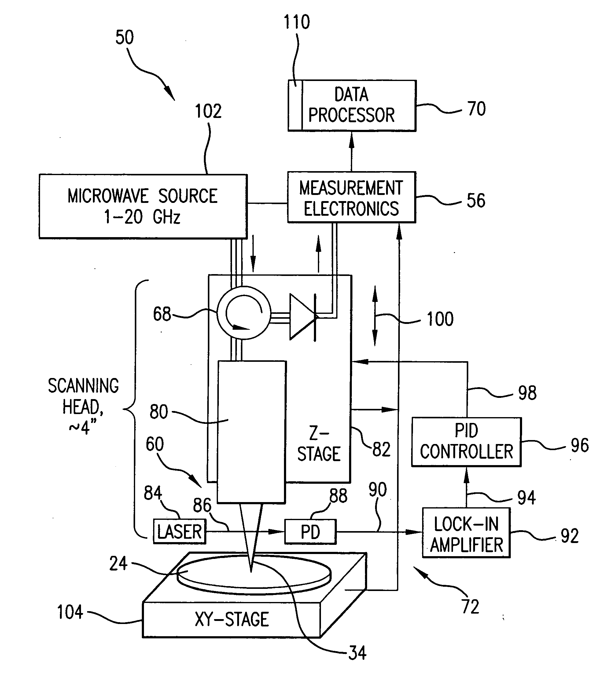
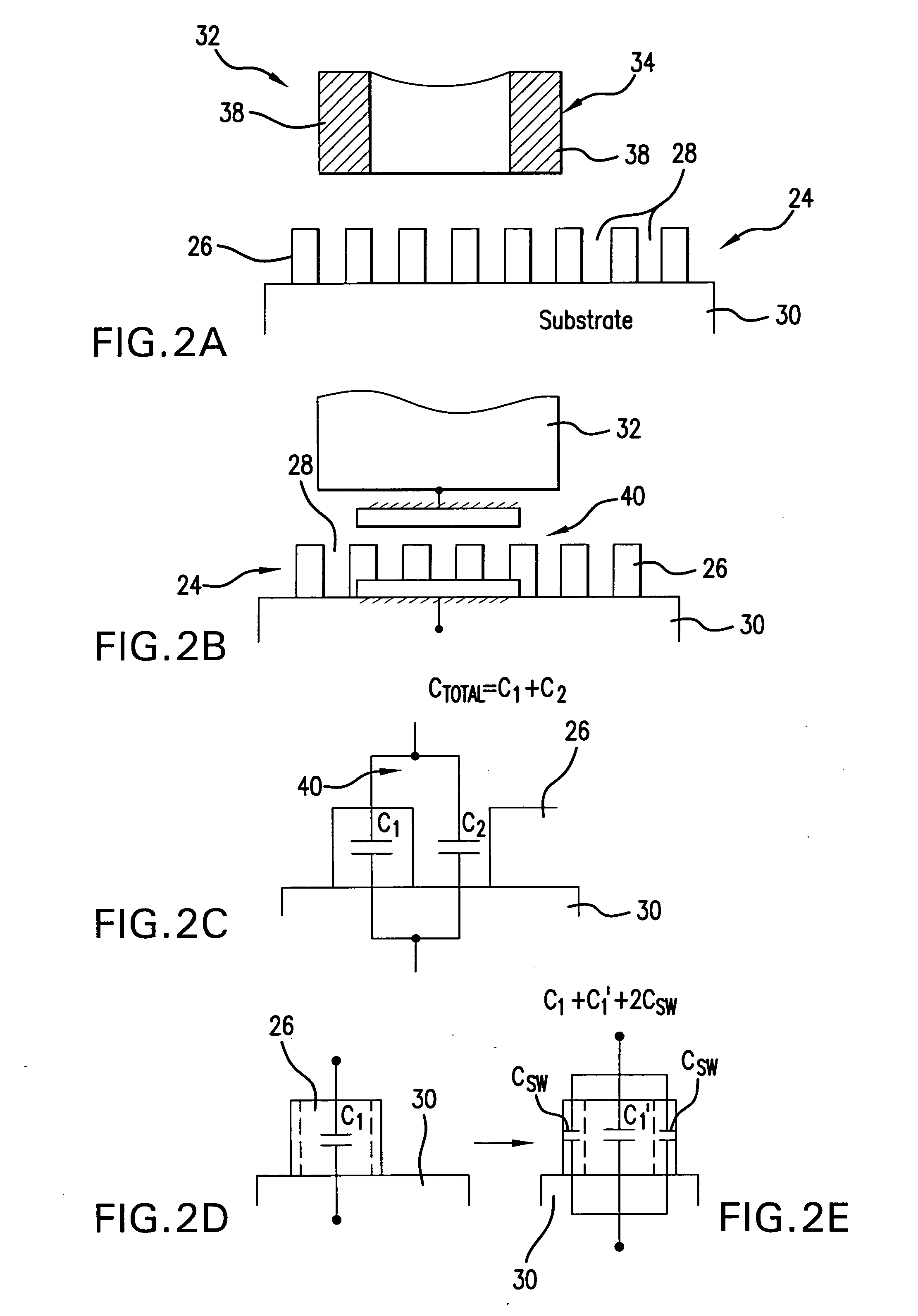
[0047] Referring to FIGS. 2A-2E, the structure (also referred to herein as a sample) under test 24 includes a low-k film 26 patterned by the Damascene process, shown in FIGS. 1A-1C, to form a plurality of trenches 28 which are parallel etched trenches formed on a substrate 30. A near field probe 32, to be discussed in further detail in following paragraphs, includes a tip 34 formed of a dielectric 36 with two metal electrodes 38 preferably formed of Al. In general, the dimensions of the probe 32 are much larger than the thickness tfilm of the dielectric film 26 and the pitch of the etched sample under test 24. Therefore, each of the electrodes 38 of the probe 32 forms a parallel plate capacitor 40 with the substrate 30 under the film 26. In order to analyze the structure presented in FIG. 2B, the equivalent scheme (or a model) involving a single pitch of the sample under test 24 is presented in FIG. 2C, where

C total=C1+C2  (1)

[0048] wherein C1 includes the effect of the sidewall d...


PUM


Abstract

By using techniques for near field probes to measure dielectric values of blanket films, the measure of the sidewall damage of the patterned structure is calculated. The interaction between the near field probe and the etched structure is modeled to obtain the model total capacitance. The near field microwave probe is calibrated on a set of blanket films with different thicknesses, and the dielectric constant of the etched trench structure is calculated using the measured frequency shift and calibration parameters. The measured capacitance is further calculated for the etched trench structure using the dielectric constant and the total thickness of the etched trench structure. The effective dielectric constant of the structure under study is extracted where the model capacitance is equal to the measured capacitance. The measure of the sidewall damage is further calculated using the effective dielectric constant.

Description

REFERENCE TO RELATED APPLICATIONS [0001] This Utility Patent Application is based on Provisional Patent Application Ser. No. 60 / 618,574, filed 15 Oct. 2004.FIELD OF THE INVENTION [0002] The present invention relates to measurement techniques. In particular, this invention directs itself to a technique for measurement of dielectric constants of etched thin films using near field microwave probes. [0003] More in particular, the present invention is directed to non-contact, non-destructive, and non-invasive measurements employing a balanced two conductor near field microwave probe to measure the extent of dielectric sidewall damage caused by the dielectric etching process used in integrated circuits fabrication. [0004] The present invention is also directed to a technique for measurements of patterned dielectric structures using quantitative dielectric constant measurements on low-k blanket films. BACKGROUND OF THE INVENTION [0005] In manufacturing of integrated circuits, the Damascene...

Claims


Application Information

Patent Timeline
IPC IPC(8): G01N27/00
CPCB82Y10/00B82Y20/00B82Y35/00G01Q60/22H01L2924/0002H01L22/12H01L2924/00
Inventor TALANOV, VLADIMIR V.SCHWARTZ, ANDREW R.SCHERZ, ANDRE
Owner SEMICON PHYSICS LAB
Why Eureka
Try Eureka