Semi-conductor component, as well as a process for the in-or output of test data

a semi-conductor and memory component technology, applied in the field of semi-conductor components, can solve the problems of inability to eject test data stored on the test data registers of each semi-conductor memory component, inability to support the protocol of the respective data buffer components used to read control signals above test data, and correspondingly similar problems

Active Publication Date: 2006-04-27
POLARIS INNOVATIONS
View PDF3 Cites 75 Cited by
  • Summary
  • Abstract
  • Description
  • Claims
  • Application Information

AI Technical Summary

Benefits of technology

[0025] The invention is aimed at providing a novel semi-conductor component, as well as a nove

Problems solved by technology

If, for example, the above buffered memory modules (“buffered DIMMs”) are subjected to an appropriate module test, the problem could occur that the above test data read control signal would not be supported by the protocol of the respective data buffer components us

Method used


Image

  • Semi-conductor component, as well as a process for the in-or output of test data
  • Semi-conductor component, as well as a process for the in-or output of test data
  • Semi-conductor component, as well as a process for the in-or output of test data

Examples


Embodiment Construction

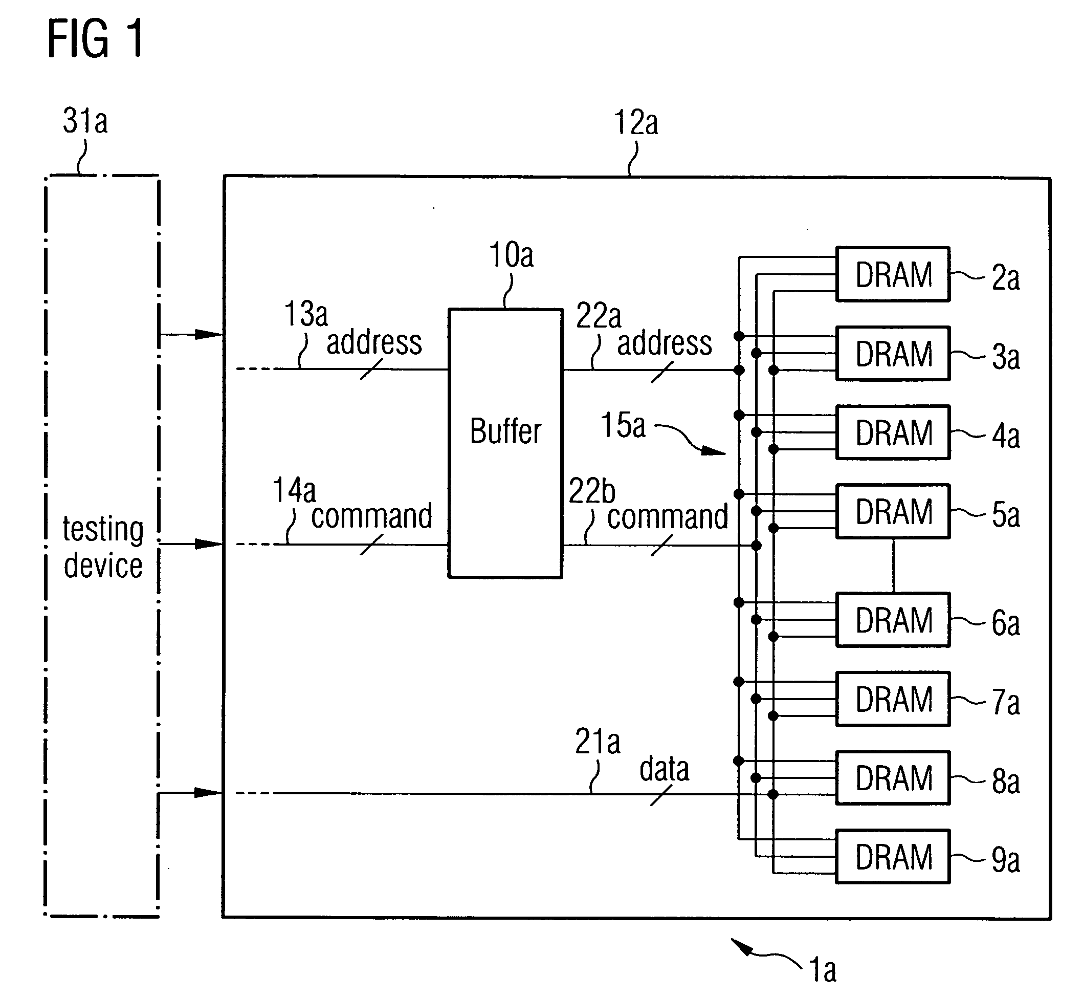
[0036] In FIG. 1 a schematic representation of a “partially” buffered memory module 1a is shown (here: a “buffered DIMM”1a), in which—as an example—a test data in- and / or output procedure in terms of an embodiment example of the invention can be used.

[0037] As is apparent from FIG. 1, the memory module 1a illustrated there comprises a plurality of memory components 2a, 3a, 4a, 5a, 6a, 7a, 8a, 9a, and—connected in series in front of the memory components 2a, 3a, 4a, 5a, 6a, 7a, 8a, 9a—one or several data buffer components (“buffers”) 10a.

[0038] The memory components 2a, 3a, 4a, 5a, 6a, 7a, 8a, 9a may be function memory or table memory components (e.g. ROMs or RAMs), especially DRAMs, e.g. DDR and / or DDR2-DRAMs, etc.

[0039] As is apparent from FIG. 1, the memory components 2a, 3a, 4a, 5a, 6a, 7a, 8a, 9a may be arranged on the same printed circuit board 12a as the buffer 10a.

[0040] The buffers 10a may for instance be appropriate Jedec-standardized (“registered DIMM”) DRAM, especiall...


PUM


Abstract

The invention relates to a semi-conductor component, and a process for the in- and/or output of test data and/or semi-conductor component operating control data into or from a semi-conductor component, whereby the semi-conductor component comprises one or more useful data memory cells, and/or one or more test data and/or semi-conductor component operating control data registers for storing test data and/or semi-conductor component operating control data, and whereby the process comprises the steps of applying a control signal to the semi-conductor component, whereby the semi-conductor component is switched from a first to a second operating mode; and applying an address signal to the semi-conductor component, whereby one or more of the test data and/or semi-conductor component operating control data registers of the semi-conductor component is addressed by the address signal in the second operating mode, and one or more of the useful data memory cells in the first operating mode.

Description

CLAIM FOR PRIORITY [0001] This application claims the benefit of priority to German Application No. 10 2004 051 345.7 which was filed in the German language on Oct. 21, 2004, the contents of which are hereby incorporated by reference. TECHNICAL FIELD OF THE INVENTION [0002] The invention relates to a semi-conductor component, as well as to a process for the in- or output of test data. BACKGROUND OF THE INVENTION [0003] Semi-conductor components, e.g. corresponding integrated (analog and / or digital) computing circuits, semi-conductor memory components such as for instance function memory components (PLAs, PALs, etc.) and table memory components (e.g. ROMs or RAMs, particularly SRAMs and DRAMs), etc. are subjected to numerous tests in the course of the manufacturing process. [0004] For the simultaneous manufacture of a plurality of (generally identical) semi-conductor components, a so-called wafer (i.e. a thin disk consisting of monocrystalline silicon) is used. The wafer is appropria...

Claims


Application Information

Patent Timeline
IPC IPC(8): G11C7/00
CPCG11C29/1201G11C29/48G11C2029/1208G11C2029/1806
Inventor BUCKSCH, THORSTENPERNER, MARTINKILIAN, VOLKERMEIER, MARTIN
Owner POLARIS INNOVATIONS
Why Eureka
Try Eureka