Semiconductor device and a method for manufacturing of the same
Inactive Publication Date: 2006-05-04
RENESAS ELECTRONICS CORP
View PDF12 Cites 36 Cited by
Summary
Abstract
Description
Claims
Application Information
AI Technical Summary
This helps you quickly interpret patents by identifying the three key elements:
Problems solved by technology
Method used
Benefits of technology
Benefits of technology
[0016] Advantageous effects obtained by the representative ones of the inventions disclosed in the present application will be explained in brief as follows:
[0017] Since the encapsulating resin is charged even below the outer peripheral portion of the back surface of the semiconductor chip, the reliability of the semiconductor device can be enhanced.
[0018] Since the area of junction between the semiconductor chip and the encapsulating resin increases, the adhesion of the encapsulating resin can be improved and the production yield of the semiconductor device can be enhanced.
Problems solved by technology
When an adhesive flows out onto the electrodes of the wiring board where the semiconductor chip is fixed to the wiring board by the adhesive, failures in the connection of bonding wires to the electrodes apt to occur, thereby causing a possibility that the reliability of electrical connection between the electrodes of the wiring board and the bonding wires will be degraded.
There is a possibility that the degradation of adhesion of the encapsulating resin will reduce reliability and production yields of the semiconductor device (semiconductor package).
Method used
Image
Click on the blue label to locate the original text in one second.
Reading with bidirectional positioning of images and text.
Examples
first preferred embodiment
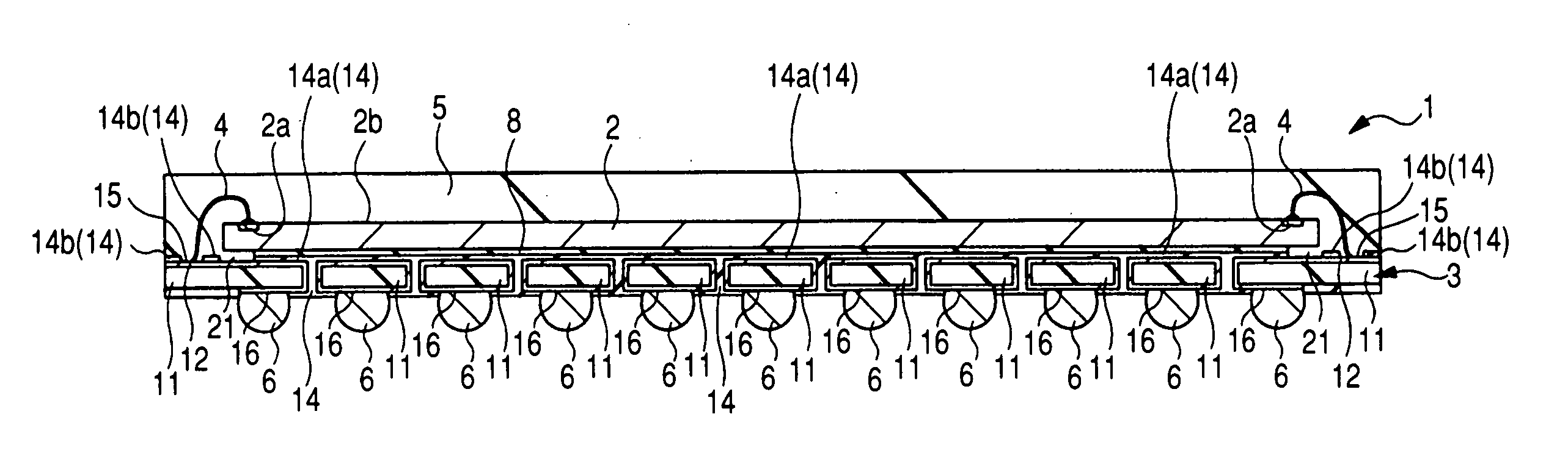
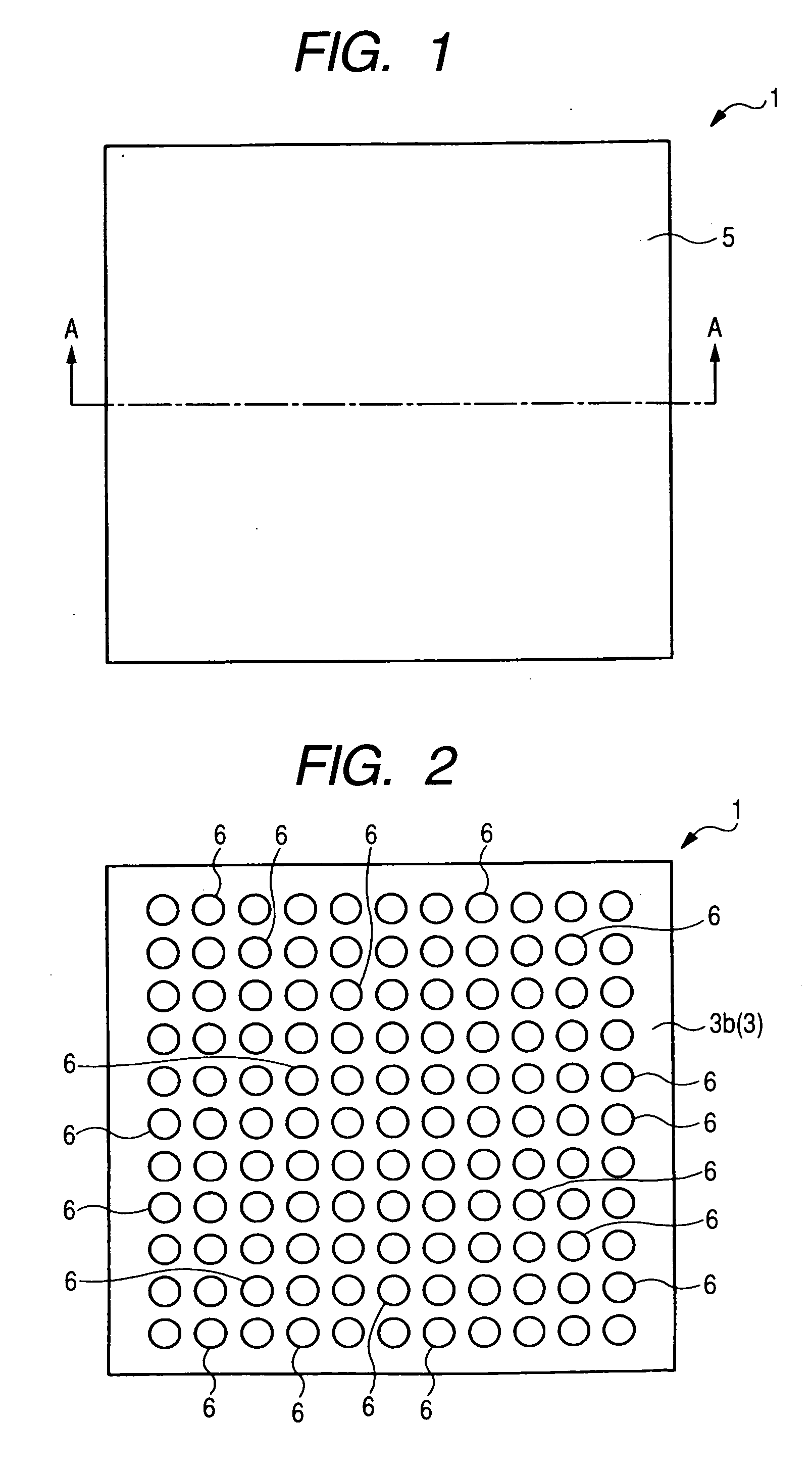
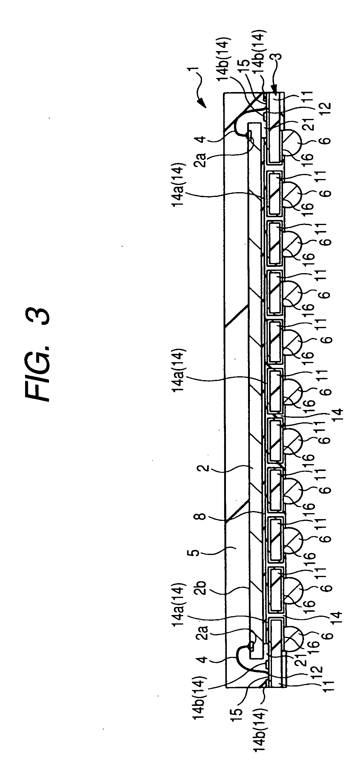
[0072] A semiconductor device according to the present embodiment and its manufacturing process will be explained with reference to the accompanying drawings.
[0073]FIG. 1 is a top view of the semiconductor device 1 showing the first embodiment of the present invention, FIG. 2 is a bottom view thereof, FIG. 3 is a sectional view (overall sectional view) thereof, FIG. 4 is a fragmentary sectional view (partly enlarged sectional view) thereof, and FIG. 5 is a side view thereof, respectively. A section taken along line A-A of FIG. 1 substantially corresponds to FIG. 3, and an enlarged view of an end nearby area of FIG. 3 substantially corresponds to FIG. 4. FIG. 6 is a plan perspective view (top view) of the semiconductor device 1 as seen through an encapsulating resin 5, and FIG. 7 is a plan perspective view (top view) of the semiconductor device 1 as seen through the encapsulating resin 5, a semiconductor chip 2 and bonding wires 4, that is, a top view of a wiring board 3 employed in...
second preferred embodiment
[0118]FIG. 30 is a fragmentary sectional view in the process of manufacturing a semiconductor device 1b showing a second embodiment of the present invention. An area substantially corresponding to FIG. 4 of the first embodiment is shown therein. FIGS. 31 and 32 are respectively explanatory views (fragmentary sectional views) of a wire bonding process employed in the present embodiment.
[0119] Since the process of manufacturing the semiconductor device 1b according to the present embodiment is substantially similar to the first embodiment except for the wire bonding process, its description will be omitted. The wire bonding process in the process of manufacturing the semiconductor device 1b according to the present embodiment will be described.
[0120] In the first embodiment, one ends of the bonding wires 4 are previously connected (first bonded) to their corresponding electrodes 2a of the semiconductor chip 2, and thereafter the other ends thereof are connected (second bonded) to th...
third preferred embodiment
[0127]FIG. 34 is a fragmentary sectional view of a semiconductor device 1c showing a third embodiment of the present invention, and FIG. 35 is a plan perspective view (top view) thereof, respectively. FIG. 34 corresponds to FIG. 4 showing the first embodiment. FIG. 35 corresponds to FIG. 7 showing the first embodiment. A plan perspective view (top view) of the semiconductor device 1c as seen through an encapsulating resin 5, a semiconductor chip 2 and bonding wires 4, i.e., a top view of a wiring board 3 employed in the semiconductor chip 1c is shown in FIG. 35. Incidentally, the outer shape of the semiconductor chip 2 is indicated by a dotted line in FIG. 35. Although FIG. 35 is a plan view, hatching is applied to each of a first solder resist section 14a, a second solder resist section 14b, a third solder resist section 14c, and connecting terminals 15 exposed from aperture parts or openings 19 of the second solder resist section 14b in order to provide easy understanding.
[0128] ...
PUM
Abstract
A first solder resist section and a second solder resist section are formed over an upper surface of a wiring board. A semiconductorchip is bonded onto the first solder resist section via an adhesive interposed therebetween. Electrodes of the semiconductorchip are respectively electrically connected to connecting terminals exposed through openings of the second solder resist section via bonding wires. An encapsulating resin is formed over the upper surface of the wiring board so as to cover the semiconductorchip and the bonding wires. A plane dimension of the first solder resist section is smaller than that of the semiconductor chip, and the encapsulating resin is filled even below an outer peripheral portion of a back surface of the semiconductor chip.
Description
CROSS-REFERENCE TO RELATED APPLICATION [0001] The present application claims priority from Japanese patent application No. 2004-315998 filed on Oct. 29, 2004, the content of which is hereby incorporated by reference into this application. BACKGROUND OF THE INVENTION [0002] The present invention relates to a semiconductor device and a manufacturing technique thereof, and particularly to a semiconductor device wherein at least one semiconductor chip is mounted over a wiring board, and a technique effective if applied to a manufacturing technique thereof. [0003] A semiconductor chip is mounted over a wiring board, electrodes of the semiconductor chip and connecting terminals of the wiring board are electrically connected to one another by bonding wires respectively, the semiconductor chip and the bonding wires are sealed with a resin, and solder balls are respectively connected to the back surface of the wiring board, whereby a semiconductor device of a semiconductor package form is ma...
Claims
Application Information
Patent Timeline
Application Date:The date an application was filed.
Publication Date:The date a patent or application was officially published.
First Publication Date:The earliest publication date of a patent with the same application number.
Issue Date:Publication date of the patent grant document.
PCT Entry Date:The Entry date of PCT National Phase.
Estimated Expiry Date:The statutory expiry date of a patent right according to the Patent Law, and it is the longest term of protection that the patent right can achieve without the termination of the patent right due to other reasons(Term extension factor has been taken into account ).
Invalid Date:Actual expiry date is based on effective date or publication date of legal transaction data of invalid patent.

