Power supply noise reduction circuit and power supply noise reduction method

a power supply and noise reduction technology, applied in the direction of dc circuit to reduce harmonics/ripples, pulse manipulation, pulse technique, etc., can solve the problems of reducing the design margin, analog circuit to malfunction, delay of the path itself changing depending, etc., to reduce the noise of the power supply

Inactive Publication Date: 2006-05-04
NEC CORP
View PDF9 Cites 22 Cited by
  • Summary
  • Abstract
  • Description
  • Claims
  • Application Information

AI Technical Summary

Benefits of technology

[0017] In view of the foregoing and other exemplary problems, drawbacks and disadvantages, it is an exemplary feature of the present invention to provide a power supply noise reduction circuit and a power supply noise reduction method that can reduce power supply noise at any frequency.
[0018] To solve the exemplary and other problems described above, a power supply noise reduction circuit according to the present invention is a power supply noise reduction circuit for reducing noise generated in a power supply comprising the power supply, a resonance circuit, and a filter.

Problems solved by technology

Today, as LSI (Large scale integration circuit) chips get faster, power supply noise reduces the margin of the design of delay, sometimes causing an analog circuit to malfunction.
Such a power supply fluctuation, if any, could change the delay amount of a gate in a logical path and, as a result, the delay of the path itself changes depending upon the amount of power supply fluctuation.
However, when the power supply fluctuation amount cannot be suppressed to a desired value, the delay margin is decreased and, in the worst case, there is no window available for use in transmission.
Therefore, if this medium potential changes, the behavior of the circuit itself changes with a possibility that the circuit does not operate as designed.
However, to allow this decoupling capacitor with the capacitance of a gate to process noise including a high-frequency noise, there is a tradeoff between the necessity to reduce the gate length and the decrease in the capacitance efficiency per unit area.
On the other hand, an increase in the on-chip capacitors results in an increase in the chip size and increases the chip cost.
However, according to the invention disclosed in Patent Document 1, it is difficult to design filtering for power supply noise unless the noise components are known, which is usually difficult to predict.
Actually, however, because a noise includes many frequency components and what frequency noise affects an LSI depends on the LSI operation, it is difficult to predict it in the design stage.
Therefore, an exemplary problem is that the noise cannot be decreased sufficiently.
Patent Documents 2-4 also fails to disclose means for solving this problem.

Method used


Image

  • Power supply noise reduction circuit and power supply noise reduction method
  • Power supply noise reduction circuit and power supply noise reduction method
  • Power supply noise reduction circuit and power supply noise reduction method

Examples


first exemplary embodiment

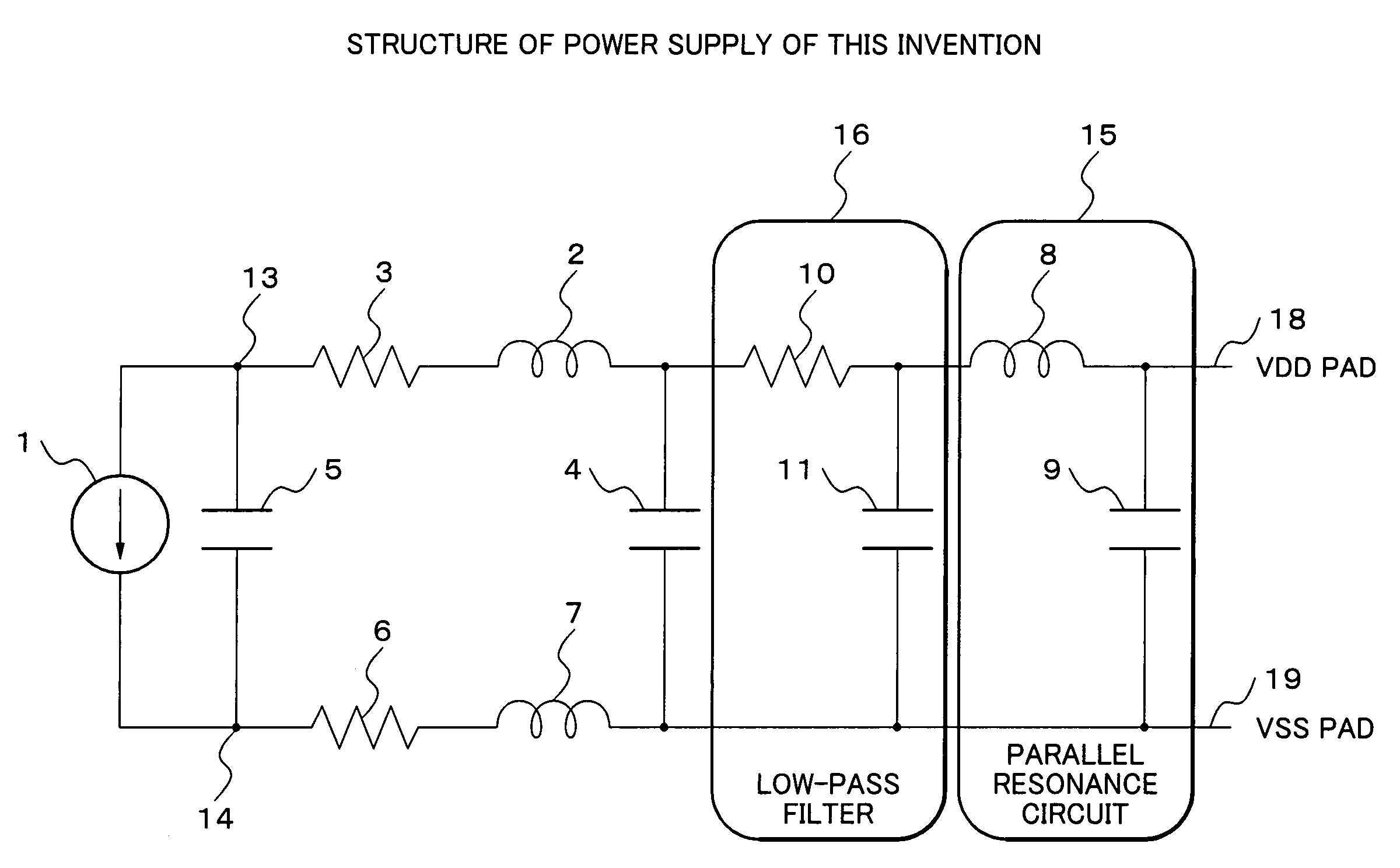
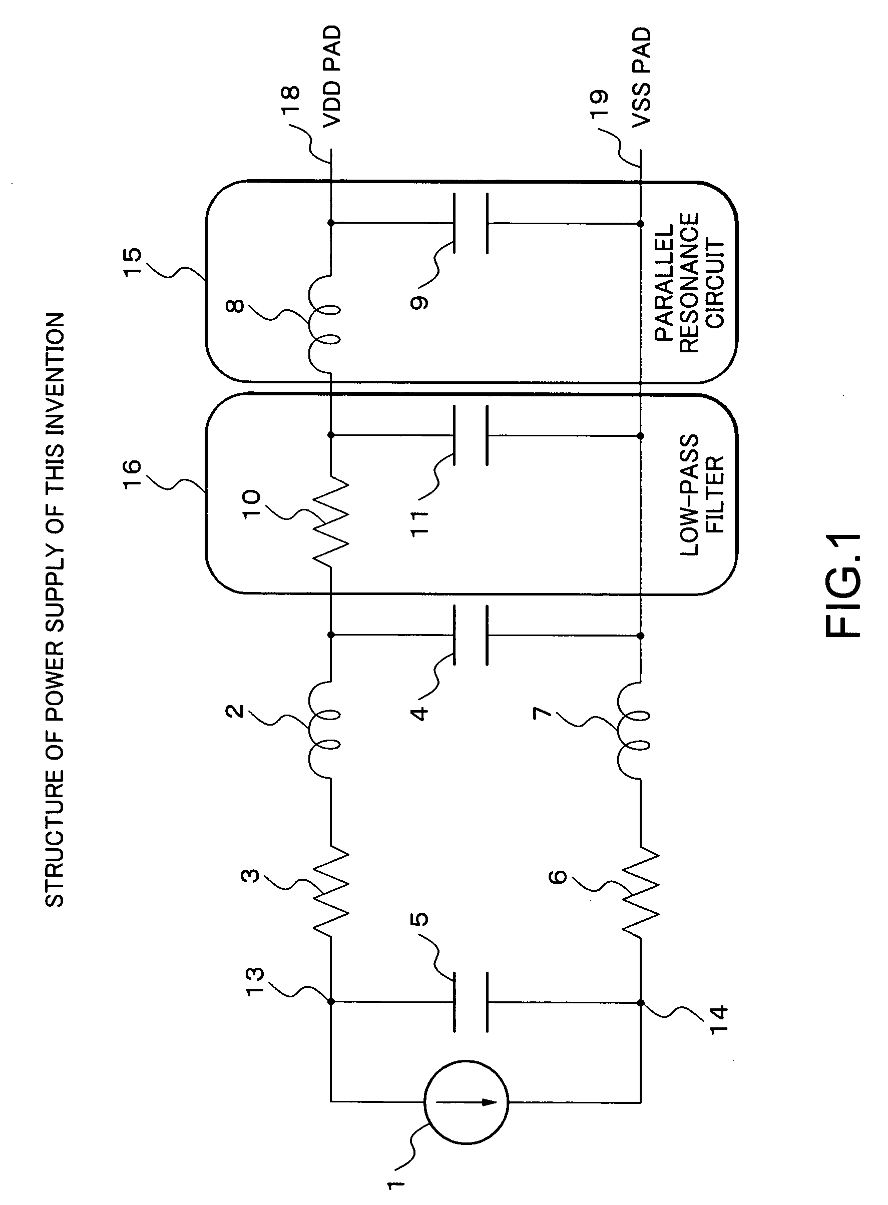
[0042]FIG. 1 is a circuit diagram showing an example of a power supply unit including a power supply noise reduction circuit according to the present invention, and FIG. 11 is a circuit diagram showing an example of a conventional power supply unit.

[0043] First, an example of a conventional power supply unit will be described. As shown in FIG. 11, the example of a conventional power supply unit comprises a current source 1, an inductor 2, a resistor 3, a capacitor 4, a capacitor 5, a resistor 6, and an inductor 7. This power supply unit further comprises a VDD pad (positive voltage output terminal) 18 and a VSS pad (negative voltage output terminal) 19.

[0044] The resistor 3 and the inductor 2 are connected in series between a terminal 13 of the current source 1 and the VDD pad 18, and the resistor 6 and the inductor 7 are connected in series between a terminal 14 of the current source 1 and the VSS pad 19.

[0045] In addition, the capacitor 5 is connected between the terminal 13 an...

second exemplary embodiment

[0075]FIG. 7 is a diagram showing an example in which resonance generators are arranged among power supply (VDD) pads 18 and GND (VSS) pads 19 in an LSI chip. As shown in the figure, the power supplies are arranged in a grid form in an LSI chip. Although the series resonance circuit disclosed in Patent Document 1 described above cannot be inserted into such a circuit, the power supply noise reduction circuit according to the present invention can be inserted.

[0076]FIG. 7 shows an example in which the parallel resonance circuits 15 in the first embodiment are arranged among a plurality of power supply (VDD) pads 18 and GND (VSS) pads 19 in an LSI chip, one parallel resonance circuit for each plurality of VDD and VSS pads. Although not shown in FIG. 7, the low-pass filter 16 in the first embodiment is inserted in series with the parallel resonance circuit in the actual configuration.

[0077]FIG. 14 is a cross section diagram showing an example in which the resonance generation circuit...

third exemplary embodiment

[0080]FIG. 8 is a configuration diagram showing an example in which the power supply noise reduction circuit according to the present invention is applied to a macro circuit. A “macro circuit” refers to a circuit block with a special function that is built in a chip, such as a RAM (random access memory) circuit or a SerDes (serial-deserial) circuit.

[0081] Referring to FIG. 8, a parallel resonance circuit 32, a low-pass filter 33, and a macro circuit 31 are connected in series to a power supply not shown. The parallel resonance circuit 32 has the same configuration as that of the parallel resonance circuit 15 in the first exemplary embodiment, and the low-pass filter 33 has the same configuration as that of the low-pass filter 16 in the first embodiment.

[0082] With the macro circuit 31 arranged as shown in FIG. 8, this power supply noise reduction circuit (parallel resonance circuit 32+low-pass filter 33) is inserted between the macro circuit 31 and an external power supply as if i...


PUM


Abstract

A power supply noise reduction circuit and a power supply noise reduction method for reducing power supply noise at any frequency, includes forcing a power supply noise to resonate to the resonance frequency of a parallel resonance circuit, including an inductor and a capacitor to set the frequency of the noise equal or close to the resonance frequency of the parallel resonance circuit and, attenuating the noise, set equal or close to the resonance frequency of the parallel resonance circuit, using a low-pass filter including a resistor and a capacitor.

Description

BACKGROUND OF THE INVENTION [0001] 1. Field of the Invention [0002] The present invention relates to a power supply noise reduction circuit and a power supply noise reduction method, and more particularly to a power supply noise reduction circuit and a power supply noise reduction method that reduce power supply noise generated by switching a current source. [0003] 2. Description of the Related Art [0004] Today, as LSI (Large scale integration circuit) chips get faster, power supply noise reduces the margin of the design of delay, sometimes causing an analog circuit to malfunction. [0005] More specifically, a current flow, which is generated each time a transistor such as a CMOS (Complementary metal oxide semiconductor) is switched on or off, causes a fluctuation in the power supply. Such a power supply fluctuation, if any, could change the delay amount of a gate in a logical path and, as a result, the delay of the path itself changes depending upon the amount of power supply fluctu...

Claims


Application Information

Patent Timeline
Patent Type & Authority Applications(United States)
IPC IPC(8): H02M1/12H03K19/00
CPCH01L23/5286H01L2224/16H01L2924/3011H03H11/126H04B1/1036H01L2224/05573H01L2224/05568H01L2924/00014H01L2224/0554H01L2224/05599H01L2224/0555H01L2224/0556
Inventor KAJITA, MIKIHIRO
Owner NEC CORP
Why Eureka
Try Eureka