Method for designing wiring connecting section and semiconductor device

a technology for connecting sections and semiconductor devices, applied in the direction of computer aided design, basic electric elements, instruments, etc., can solve the problems of reducing the degree of freedom in designing wirings, deteriorating electrical characteristics, and lowering fabrication yield, so as to improve the degree of freedom in wiring design, reduce the cost, and improve the integration of semiconductor devices

Inactive Publication Date: 2006-05-11
FUJITSU MICROELECTRONICS LTD
View PDF24 Cites 3 Cited by
  • Summary
  • Abstract
  • Description
  • Claims
  • Application Information

AI Technical Summary

Benefits of technology

[0015] An object of the present invention is to provide a method for designing a wiring connecting section, which is capable of improving a degree of freedom in designing a wiring while satisfying electrical specifications required for the wiring connecting section, and to provide a semiconductor device having a wiring connecting section designed by the method for designing a wiring connecting section.
[0023] In the present invention, since the number and the position of stack vias are determined as described above, not only electrical demands in the connecting section between the first wiring and the second wiring can be satisfied, but also other wirings can be passed between the stack vias, and thus the degree of freedom in designing the wirings is enhanced to a great extent as compared with the conventional one. Thus, cost reduction due to reduction of the number of wiring layers and much higher integration of the semiconductor device can be realized.
[0026] As described above, the wiring is passed between the stack vias, thus the degree of freedom in designing the wirings is increased, and cost reduction due to reduction of the number of wiring layers and much higher integration of the semiconductor device can be realized.

Problems solved by technology

Moreover, the design rules are determined by limitations on a fabrication process, electrical specifications required for the semiconductor device and the like.
As described above, in the conventional semiconductor device, it is necessary to arrange the other wirings so as to be detoured around the connecting regions of the broad-width wirings; therefore, the wirings are elongated, thus causing deterioration of the electrical characteristic and lowering a degree of freedom in designing the wirings.
When the degree of freedom in designing the wiring is lowered, the number of wiring layers must be further increased, thus increasing a fabrication cost and lowering fabrication yield.

Method used


Image

  • Method for designing wiring connecting section and semiconductor device
  • Method for designing wiring connecting section and semiconductor device
  • Method for designing wiring connecting section and semiconductor device

Examples


Embodiment Construction

[0035] Hereinafter, description will be made for an embodiment of the present invention with reference to the accompanying drawings.

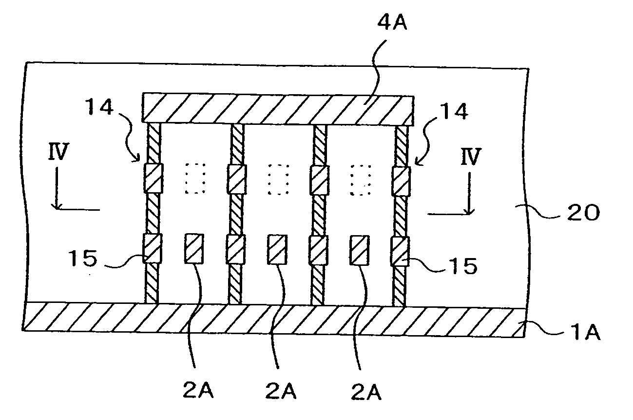
[0036]FIG. 4 is a plan view showing a wiring part of a semiconductor device according to the embodiment of the present invention, FIG. 5 is a longitudinal sectional view taken along a line III-III of FIG. 4, and FIG. 6 is a transverse sectional view taken along a line IV-IV of FIG. 5. Note that illustration of an insulating layer and a semiconductor substrate below and under wiring 1A is omitted in FIG. 5.

[0037]FIG. 4 shows four wiring layers stacked on a semiconductor substrate 10 having specified elements (cells) formed thereon with an insulating layer interposed thereamong. Note that, though FIG. 4 shows only the four wiring layers, other wiring layers may be formed above or below these wiring layers.

[0038] In this embodiment, these four wiring layers are referred to as a first wiring layer, a second wiring layer, a third wiring layer and a fourth...


PUM


Abstract

First, an amount of a current flowing between a first wiring and a third wiring is estimated, and the number of stack vias required for connecting the first wiring and the third wiring is determined. Next, based on the number of stack vias, the number of virtual wirings for determining positions of the stack vias is determined. Thereafter, the virtual wirings are arranged in a forming region of the third wiring above the first wiring, for example, at an equal interval, and the stack vias are created in intersections of the first wiring and the virtual wirings. Thereafter, the virtual wirings are removed, and the third wiring is created. According to needs, a second wiring passing between the stack vias is created.

Description

CROSS-REFERENCE TO RELATED APLICATIONS [0001] This application is based upon and claims priority of Japanese Patent Applications No. 2001-272228, filed in Sep. 7, 2001, the contents being incorporated herein by reference. This application is a divisional of prior application Ser. No. 10 / 097,871 filed Mar. 15, 2002.BACKGROUND OF THE INVENTION [0002] 1. Field of the Invention [0003] The present invention relates to a method for designing a wiring connecting section, in which wirings in mutually different wiring layers are electrically connected one another via a plurality of stack vias, and to a semiconductor device having a wiring connecting section designed by the method for designing a wiring connecting section. [0004] 2. Description of the Prior Art [0005] In recent years, high integration of the semiconductor device has been further accelerated, and accompanied with such acceleration, also with regard to wirings of the semiconductor device, micro-fabrication and multi-layering ha...

Claims


Application Information

Patent Timeline
Patent Type & Authority Applications(United States)
IPC IPC(8): H01L23/48G06F17/50H01L21/82H01L21/00H01L23/522
CPCG06F17/5077H01L23/5226H01L2924/0002H01L2924/00G06F30/394H01L21/00
Inventor KUMAGAI, KENJI
Owner FUJITSU MICROELECTRONICS LTD
Why Eureka
Try Eureka