Methods for fabricating compound material wafers

a technology of compound material and wafers, which is applied in the direction of basic electric elements, electrical equipment, semiconductor devices, etc., can solve the problems of high cost of adaptive steps and added process costs by designed equipment, and achieve the effect of increasing the thickness

Active Publication Date: 2006-05-11
S O I TEC SILICON ON INSULATOR THECHNOLOGIES
View PDF27 Cites 87 Cited by
  • Summary
  • Abstract
  • Description
  • Claims
  • Application Information

AI Technical Summary

Benefits of technology

[0004] Presented are methods for fabricating compound material wafers which overcome the problems of the prior art, and which enable compound material wafers to be fabricated using standard wafer processing equipment. An embodiment includes providing a donor substrate having a surface, forming a weakened zone in the donor substrate to define a transfer layer that includes the donor substrate surface, bonding the surface of the transfer layer to a handle substrate, and detaching the donor substrate at the weakened zone to transfer the transfer layer onto the handle substrate. Consequently, a compound material wafer is formed, and the transfer layer detached donor wafer provides a remainder substrate having a surface where the transfer layer was detached. Next, an additional layer is deposited onto a surface of the remainder substrate to increase its thickness and to form a reconditioned substrate, and the reconditioned substrate is recycled as a donor substrate for fabricating additional compound material wafers.

Problems solved by technology

Both of these solutions, however, require adaptive steps which are very costly.
Such specially designed equipment adds more expense to the process.

Method used


Image

  • Methods for fabricating compound material wafers
  • Methods for fabricating compound material wafers
  • Methods for fabricating compound material wafers

Examples


second embodiment

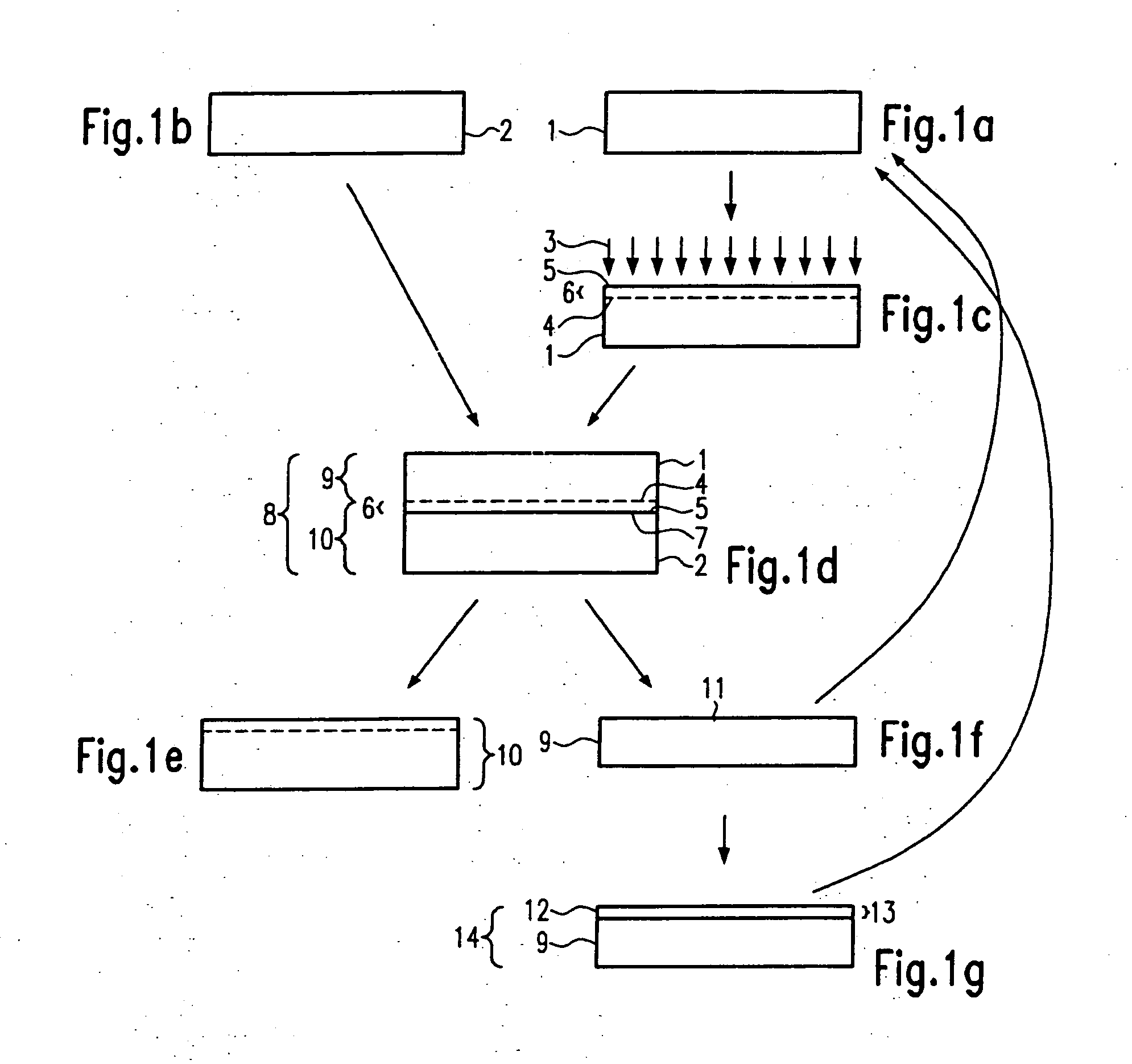
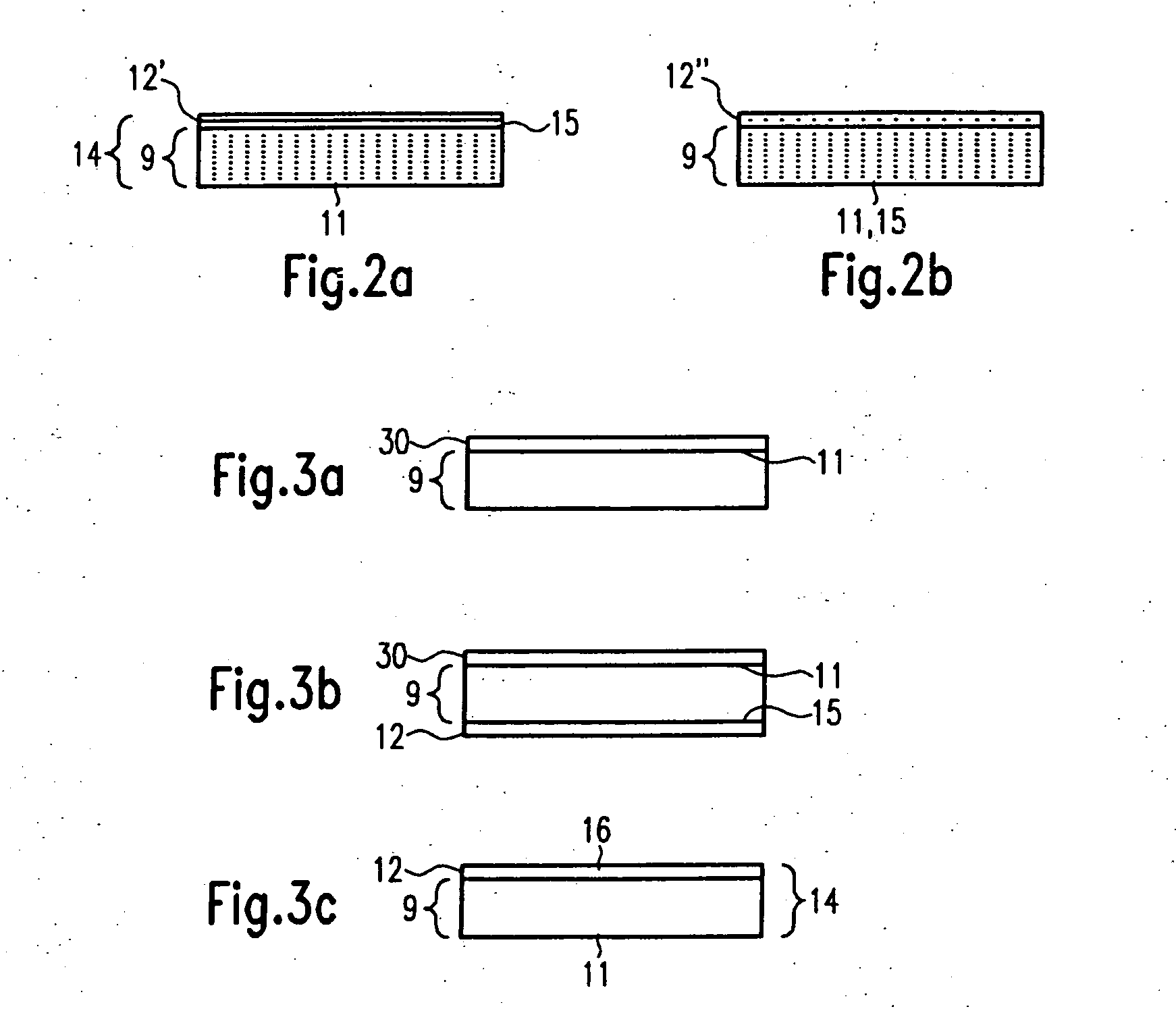
[0021]FIG. 3 illustrates the present manufacturing method in which the step illustrated in FIG. 1g is replaced by the process illustrated in FIGS. 3a to 3c. Corresponding elements and features shown in FIG. 1 have the same reference numerals, and are not explained again in detail; instead their description is incorporated by reference.

[0022] According to FIG. 3a, a protective layer 30 is deposited on the top surface 11 of the remainder substrate 9, wherein the top surface 11 is the surface at which detachment occurred. The protective layer 30 protects the top surface 11 against contamination or mechanical damage during further processing. Suitable protecting materials may include silicon dioxide or silicon nitride (Si02, Si3N4).

first embodiment

[0023] In FIG. 3b, the layer 12 is deposited on the bottom or opposite surface 15 of the remainder substrate 9. This is identical to that illustrated and described with respect to FIG. 1g of the

[0024]FIG. 3c illustrates the removal of the protective layer 30. The reconditioned donor substrate 14 includes the remainder substrate 9 and the deposited layer 12, and is then reused as an initial donor substrate 1. Eventually, removal of the protective layer 30 can be accompanied by an additional polishing and / or cleaning step of the top surface 11.

[0025] According to a further variant, after the growth of layer 12 the surface 16 of the additional layer could be provided with a further protective film to protect this surface of the reconditioned donor substrate 14 during the process steps illustrated in FIGS. 1a to 1f.

[0026] The application of the present manufacturing method is explained below in detail using the example of a compound wafer having a GaN transfer layer. Variants describe...


PUM

PropertyMeasurementUnit
thicknessaaaaaaaaaa
thicknessaaaaaaaaaa
energyaaaaaaaaaa

Abstract

Methods for fabricating compound material wafers are described. An embodiment of the method includes providing a donor substrate having a surface, forming a weakened zone in the donor substrate to define a transfer layer that includes the donor substrate surface, bonding the surface of the transfer layer to a handle substrate, and detaching the donor substrate at the weakened zone to transfer the transfer layer onto the handle substrate. Consequently, a compound material wafer is formed, and the transfer layer detached donor wafer provides a remainder substrate having a surface where the transfer layer was detached. Next, an additional layer is deposited onto a surface of the remainder substrate to increase its thickness and to form a reconditioned substrate, and the reconditioned substrate is recycled as a donor substrate for fabricating additional compound material wafers.

Description

BACKGROUND ART [0001] The present invention generally relates to methods for fabricating compound material wafers. An embodiment includes providing a donor substrate, forming a weakened zone in the donor substrate to define a transfer layer, bonding the surface of the transfer layer to a handle substrate, and detaching the donor substrate at the weakened zone to transfer the transfer layer onto the handle substrate. This forms a compound material wafer, and the transfer layer detached donor wafer provides a remainder substrate having a surface where the transfer layer was detached. Next, an additional layer is deposited onto a surface of the remainder substrate to increase its thickness and to form a reconditioned substrate, and the reconditioned substrate is recycled as a donor substrate for fabricating additional compound material wafers. [0002] Published U.S. application no. 2003 / 0153163 describes a method for transferring a layer of material from a donor substrate to a handle su...

Claims


Application Information

Patent Timeline
Patent Type & Authority Applications(United States)
IPC IPC(8): H01L21/30
CPCH01L21/02032H01L21/76254Y10S438/93Y10S438/933H01L27/12
Inventor DUPONT, FREDERIC
Owner S O I TEC SILICON ON INSULATOR THECHNOLOGIES
Why Eureka
Try Eureka