Contact image capturing structure

a technology of contact image and structure, which is applied in the direction of solid-state devices, instruments, semiconductor devices, etc., can solve the problems of image decay and distortion, the packaging structure of the detect chip cannot be further narrowed, and the image cannot be displayed originally, so as to achieve the effect of greatly reducing the volume of the packaging structur

Inactive Publication Date: 2006-05-18
ADVMATCH TECH
View PDF12 Cites 21 Cited by
  • Summary
  • Abstract
  • Description
  • Claims
  • Application Information

AI Technical Summary

Benefits of technology

[0008] It is therefore another objective of the claimed invention to provide a contact image capturing structure that the volume of the packaging structure can be greatly reduced, since the conventional optical devices are no more needed.

Problems solved by technology

However, this kind of packaging structure of the detect chip cannot be further narrowed, since size of the detect chips must cooperate with the formation distance of images.
In addition, the packaging structures utilize the refraction or diffraction principles to form the images, so that the images cannot be displayed originally.
After the refraction or diffraction processes, the images will be decayed and distorted, and the resolution of the images cannot be further improved.

Method used


Image

  • Contact image capturing structure
  • Contact image capturing structure
  • Contact image capturing structure

Examples


Embodiment Construction

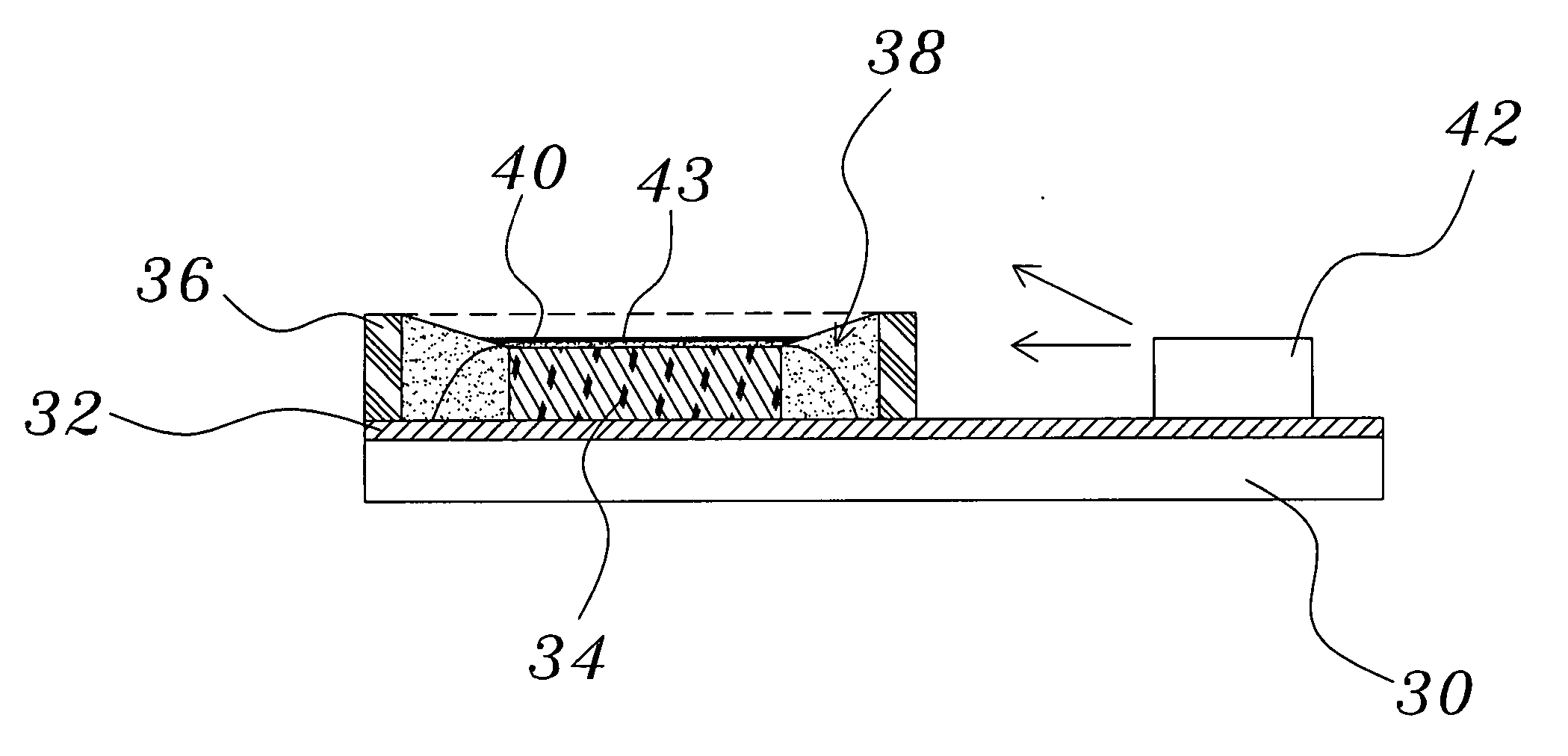
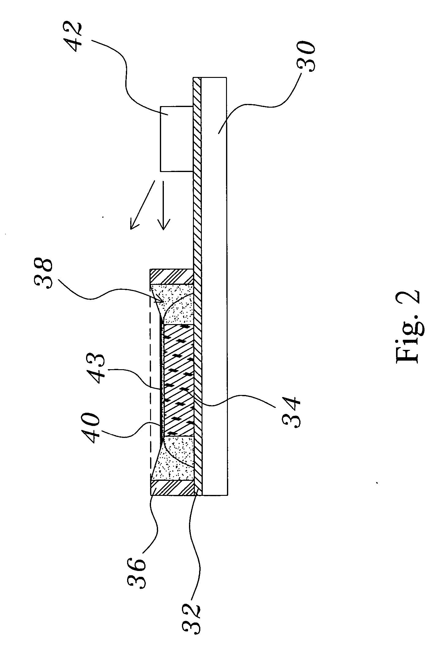
[0019] The claimed invention discloses a contact image capturing structure, and this structure can be applied to various fields, such as fingerprint identification, biosensor and derma medical monitoring. The claimed invention will be explained in detail with the embodiment of the fingerprint identifier. As shown in FIG. 2, the claimed contact image capturing structure comprises a substrate 30 having a circuit layer 32, and a detect chip 34 located on the substrate 30 and electrically connected to the circuit layer 32. Wherein the detect chip 34 is electrically connected to the circuit layer 32 by wire bonding type or flip chip type, and the detect chip 34 is selected from one of charge-coupled device (CCD) and complementary metal oxide semiconductor (CMOS). Then, a transparent frame 36 is formed on the substrate 30, and transmittance of the frame 36 is 10% to 30%. The frame 36 surrounds the detect chip 34, and a cavity 38 is formed between the frame 36 and the detect chip 34. A tra...


PUM


Abstract

The present invention provides a contact image capturing structure comprising a substrate having a circuit layer, a detect chip located on the substrate and electrically connected to the circuit layer, a frame located on the substrate and surrounding the detect chip, a cavity is formed between the frame and the detect chip, and a transparent layer located in the frame to cover the detect chip and the circuit layer. The transparent layer above the detect chip is flat and the transparent layer above the cavity is slanted. Hence, the present invention can greatly reduce volume of the chip packaging structure, since the conventional optical devices are no more required. In addition, with the directly contact detection, the detected images can be directly displayed.

Description

BACKGROUND OF INVENTION [0001] 1. Field of the Invention [0002] The invention relates to an image detecting structure, and more particularly, to a contact image capturing structure with small volume and can directly display images. [0003] 2. Description of the Prior Art [0004] As the advance of the society, the image detecting technology is applied to more and more electronic products, such as the digital camera, biosensor and fingerprint identifier. [0005] The packaging structure of the conventional detect chip is shown in FIG. 1. The conventional structure includes a substrate 10, a detect chip 12 installed on the substrate 10, a flange 14 formed on the substrate 10 and around the detect chip 12, a fillister 16 formed by the flange 14 and the substrate 10, and a plurality of conducting wires 18 electrically connecting the detect chip 12 and the substrate 10. A transparent board 20 is adhered on the flange 14 to cover the fillister 16, and the substrate 10, the transparent board 20...

Claims


Application Information

Patent Timeline
Patent Type & Authority Applications(United States)
IPC IPC(8): H01L31/0203
CPCG06K9/00053H01L27/14685H01L31/0232H01L31/147H01L31/0203H01L2224/48091G06V40/1329H01L2924/00014
Inventor CHEN, NENG CHIN
Owner ADVMATCH TECH
Why Eureka
Try Eureka