Solid state vacuum devices and method for making the same

a vacuum device and solid-state semiconductor technology, applied in the manufacture of electric discharge tubes/lamps, electrode systems, discharge tubes luminescnet screens, etc., can solve the problems of inter-electrode electron leakage, high frequency or severe environmental conditions, vacuum tubes remaining in use, etc., to achieve the effect of increasing power generation capacity

Inactive Publication Date: 2006-06-15
HWU RUEY JEN +1
View PDF4 Cites 10 Cited by
  • Summary
  • Abstract
  • Description
  • Claims
  • Application Information

AI Technical Summary

Problems solved by technology

The result is that today more circuits are utilizing solid-state semiconductor devices, with vacuum tubes remaining in use only in limited circumstances such as those involving high power, high frequency, or hazardous environmental applications.
In these limited circumstances, solid-state semiconductor devices generally cannot accommodate the high power, high frequency or severe environmental conditions.
Among the problems with this structure were inter-electrode electron leakage, electron leakage between adjacent devices, and functional cathode life.

Method used


Image

  • Solid state vacuum devices and method for making the same
  • Solid state vacuum devices and method for making the same
  • Solid state vacuum devices and method for making the same

Examples


Embodiment Construction

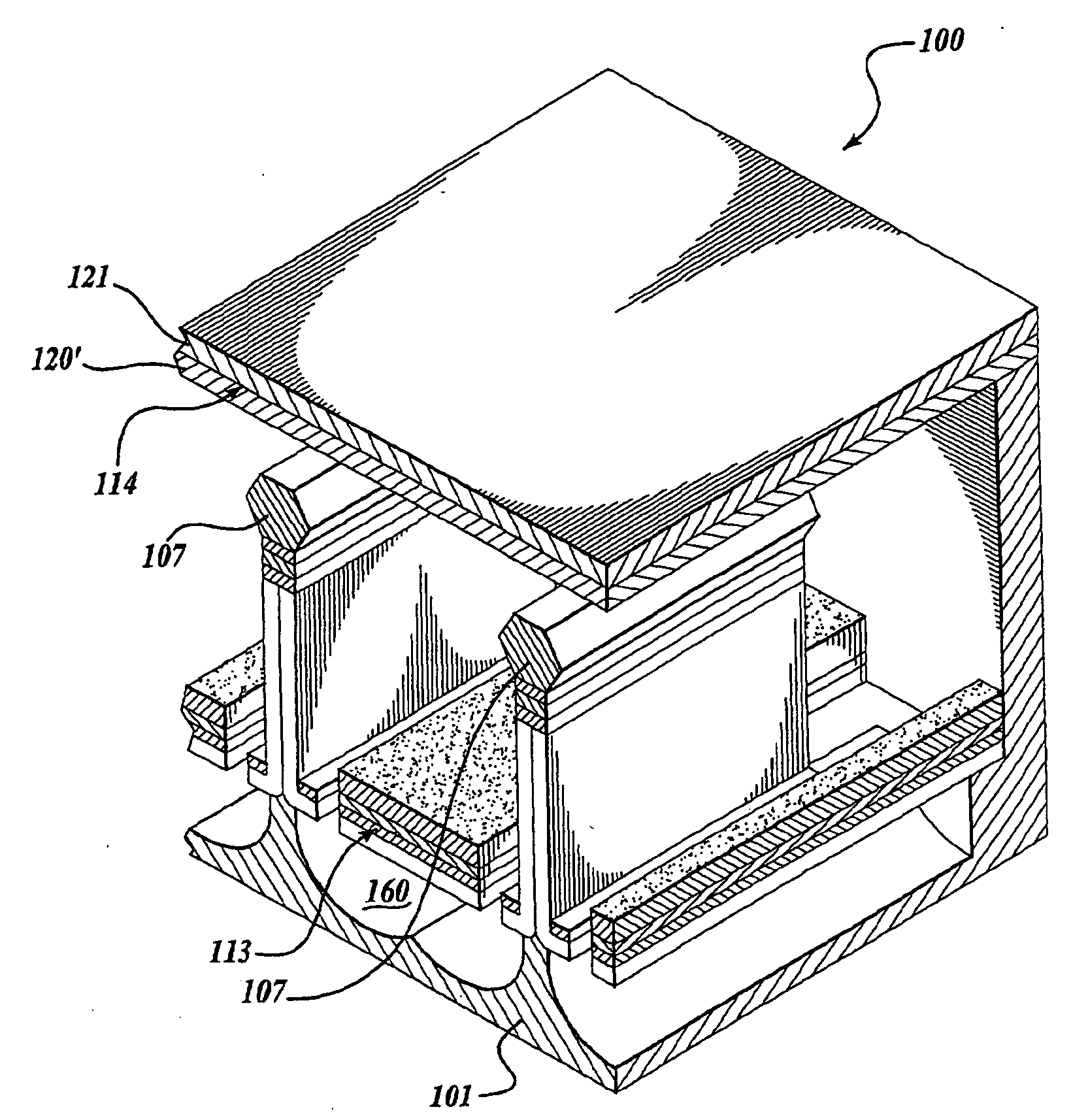
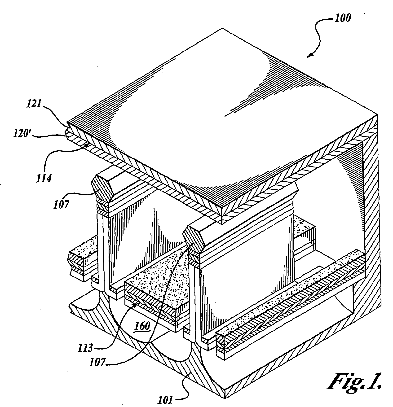
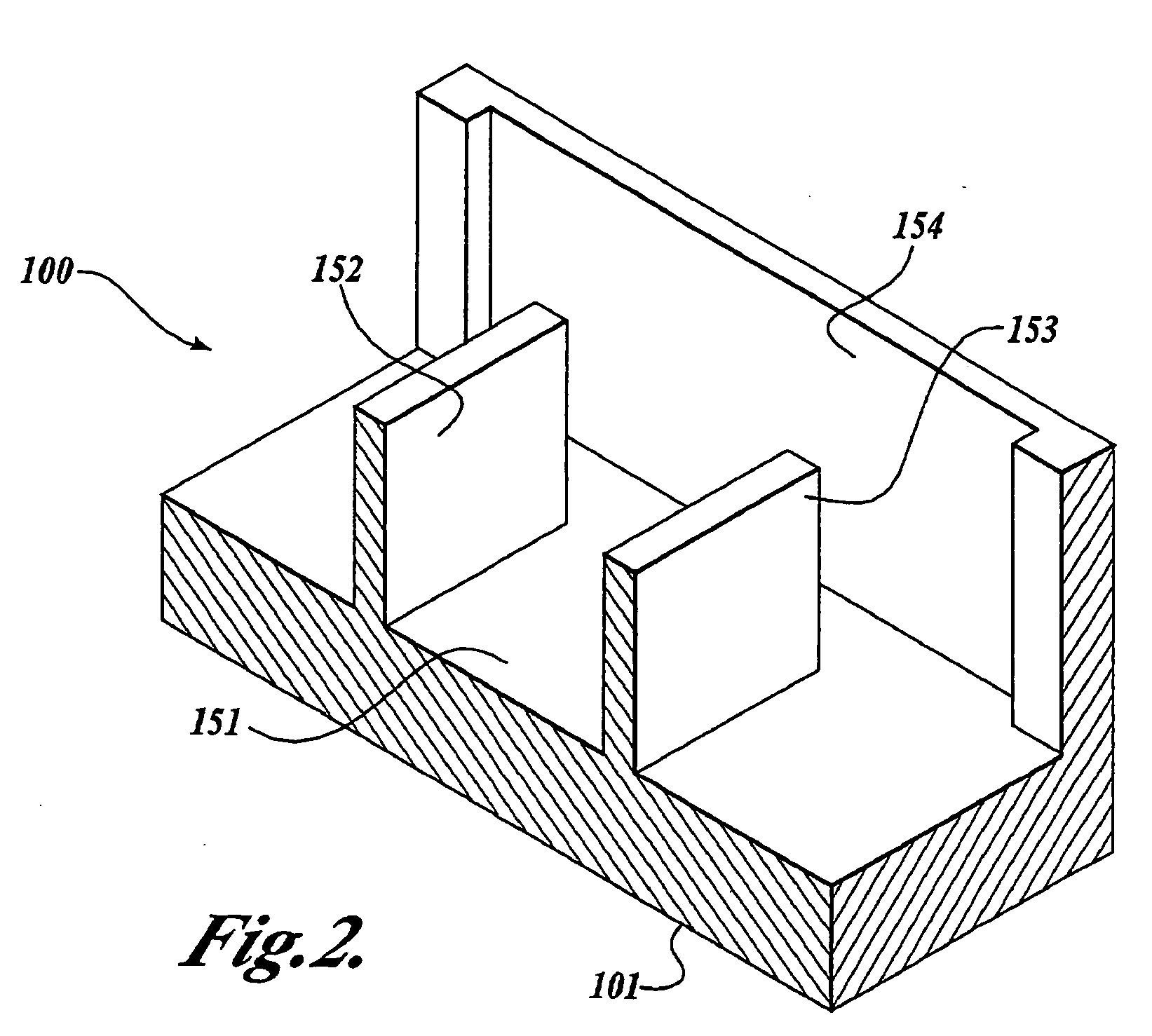
[0034] The present invention provides a sub micron-scale to cm-scale and beyond, solid-state vacuum device that operates in a manner similar to that of a traditional vacuum tube devices. As described below, the present invention includes a plurality of embodiments where a device is configured to form a diode, triode, tetrode, pentode or other higher order devices made from novel semiconductor fabrication techniques. The following sections provide a detailed description of each embodiment and several fabrication methods for making the devices disclosed herein.

[0035] Referring now to FIG. 1, the basic elements of one embodiment of a triode solid state vacuum device 100 (hereinafter referred to as the triode 100) are shown. Generally described, the triode 100 comprises a substrate 101 having a cavity 160 formed in the substrate 101. The triode 100 further comprises a cathode 113 positioned near the opening of the cavity 160. As described in detail below, the cathode 113 is in the form...


PUM


Abstract

A solid-state vacuum device (SSVD) and method for making the same. In one embodiment, the SSVD forms a triode device comprising a substrate having a cavity formed therein. The SSVD further comprises cathode positioned near the opening of the cavity, wherein the cathode spans over the cavity in the form of a bridge that creates an air gap between the cathode and substrate. In addition, the SSVD further comprises an anode and a grid that is positioned between the anode and cathode. Upon applying heat to the cathode, electrons are released from the cathode, passed through the grid, and received by the anode. In response to receiving the electrons, the anode produces a current. The current received by the anode is controlled by a voltage applied to the grid. Other embodiments of the present invention provide diode, tetrode, pentode, and other higher order device configurations.

Description

CROSS-REFERENCE TO RELATED APPLICATIONS [0001] This continuation application claims benefit of pending U.S. patent application Ser. Nos. 10 / 067,616 and 10 / 067,625, both filed contemporaneously on Feb. 4, 2002, the contents of which are incorporated herein by reference for all purposes.FIELD OF THE INVENTION [0002] The present invention relates to semiconductor devices and vacuum devices, and in particular, to devices configured to operate in a vacuum environment and devices manufactured through microelectronic, micro electromechanical systems (MEMS), micro system technology (MST), micromachining, and semiconductor manufacturing processes. BACKGROUND OF THE INVENTION [0003] Vacuum tubes were developed at or around the turn of the century and immediately became widely used for electrical amplification, rectification, oscillation, modulation, and wave shaping in radio, television, radar, and in all types of electrical circuits. With the advent of the transistor in the 1940s and 1950s a...

Claims


Application Information

Patent Timeline
Patent Type & Authority Applications(United States)
IPC IPC(8): H01J1/46H01J1/13H01J1/62H01J3/02H01J21/10
CPCH01J1/13H01J1/46H01J3/027H01J19/38H01J21/105
Inventor HWU, RUEY-JENSADWICK, LARRY
Owner HWU RUEY JEN
Why Eureka
Try Eureka