Manufacturing method of a quad flat no-lead package structure

a manufacturing method and package structure technology, applied in the direction of electrical equipment, semiconductor devices, semiconductor/solid-state device details, etc., can solve the problems of over-glue and the inability to increase and achieve the effect of increasing the i/o pad density of the package structur

Active Publication Date: 2006-06-22
UNITED MICROELECTRONICS CORP
View PDF3 Cites 0 Cited by
  • Summary
  • Abstract
  • Description
  • Claims
  • Application Information

AI Technical Summary

Benefits of technology

[0011] The present invention provides a quad flat no-lead (QFN) package structure, which affords higher I / O pad density for the package structure.
[0012] The present invention provides a fabrication process for fabricating a quad flat no-lead (QFN) package, for improving the package quality of the package structure and solving the over-glue problems.
[0015] In this invention, the conductive leads (i.e. metal blocks) are arranged on the bottom surface of the chip carrier. Compared with the prior art, there are much more conductive leads in the chip carrier due to the arrangement of the conductive leads, thus fortifying the electrical properties of the package structure.

Problems solved by technology

However, the number of the I / O pads is limited by the space occupied by the die pad, so that the I / O pad density can not be increased.
Moreover, in the molding process, a portion of the molding compound 150 may overflows to the bottom surface of the die pad 120 or the lower surfaces of the leads 140, causing the over-glue problem.

Method used


Image

  • Manufacturing method of a quad flat no-lead package structure
  • Manufacturing method of a quad flat no-lead package structure
  • Manufacturing method of a quad flat no-lead package structure

Examples


Embodiment Construction

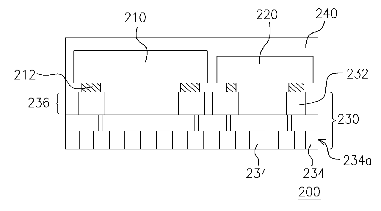
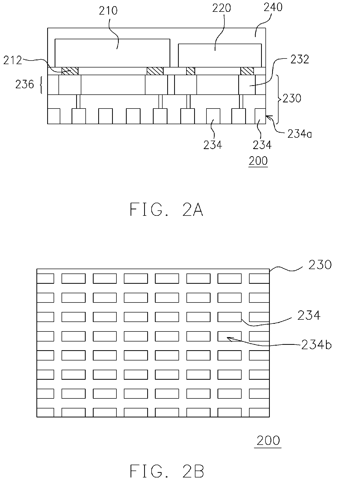
[0024] Referring to FIGS. 2A & 2B, illustrating a cross-sectional view and a bottom view of a QFN package structure according one preferred embodiment of the present invention. The package structure 200 comprises a first chip 210, a second chip 220, a chip carrier 230 and a passivation layer 240. The first chip 210 and the second chip 220 are electrically connected to the chip carrier 230 by surface mount technology (SMT), or wire bonding or flip chip technology, for example, to form the multi-chip package IC module. Taking SMT as an example, the chips 210, 220 are electrically connected to contact pads 232 of the chip carrier 230 through anisotropic conductive paste (ACP) 212. If the flip chip technology is used, the first and second chips are electrically connected to the pads 232 of the chip carrier 230 through bumps (not shown) arranged in arrays. Similarly, if the wire-bonding technology is used, the backsides of the first and second chips are attached to the chip carrier 230 a...


PUM


Abstract

The present invention provides a method for fabricating a quad flat no-lead package structure, comprising a chip carrier and at least a chip. The chip is disposed on the top surface of the chip carrier, while the back surface of the chip carrier includes a plurality of flat no-lead conductive leads as I / O pads of the chip carrier for the external circuitry. A plurality of pads, corresponding to bonding pads of the chip, is disposed on the top surface of the chip carrier. The aforementioned package structure can employ wiring bonding technology, flip chip technology or surface mount technology to attach the chip to the chip carrier.

Description

CROSS-REFERENCE TO RELATED APPLICATION [0001] This is a divisional application of application Ser. No. 10 / 710,933, filed on Aug. 13, 2004, which claims the priority benefit of Taiwan patent application serial no. 92127758, filed on Oct. 7, 2003, now pending. The entirety of each of the above-mentioned patent applications is hereby incorporated by reference herein and made a part of this specification.BACKGROUND OF THE INVENTION [0002] 1. Field of Invention [0003] The present invention relates to a manufacturing method of a package structure. More particularly, the present invention relates to a manufacturing method of a quad flat no-lead (QFN) package structure. [0004] 2. Description of Related Art [0005] The semiconductor industries are highly developed high tech industries. With the trends of electrification, electronic and semiconductor devices are widely used in the daily life, including entertainment, education, transportation and households. The design of the electrical produc...

Claims


Application Information

Patent Timeline
Patent Type & Authority Applications(United States)
IPC IPC(8): H01L23/48H01L23/498
CPCH01L23/49827H01L2224/16H01L2224/32245H01L2224/48091H01L2224/48247H01L2224/73265H01L2924/01078H01L2924/01079H01L2924/00014H01L24/48H01L2224/45144H01L2924/00H01L2924/10253H01L24/45H01L2224/05571H01L2224/05573H01L2924/14H01L2924/181H01L2224/05599H01L2924/00012
Inventor PAN, JUI-HSIANGLEE, KUANG-SHINSUN, CHENG-KUANG
Owner UNITED MICROELECTRONICS CORP
Why Eureka
Try Eureka