Anchored non-solder mask defined ball pad

a ball pad and mask technology, applied in the field of integrated circuits, can solve the problems of smd pad being a material mismatch at the junction between the solder ball and the solder ball, affecting the placement and alignment of the components on the circuit board, and affecting the accuracy of the placement and alignment of the components

Inactive Publication Date: 2006-06-22
STMICROELECTRONICS SRL
View PDF3 Cites 85 Cited by
  • Summary
  • Abstract
  • Description
  • Claims
  • Application Information

AI Technical Summary

Problems solved by technology

With small pads and tight spacing, the precision of the placement and alignment of the component on the circuit board becomes critical.
Second, because the copper needs to extend beyond the edge of the solder mask the actual copper pad area is larger.
The drawback

Method used


Image

  • Anchored non-solder mask defined ball pad
  • Anchored non-solder mask defined ball pad
  • Anchored non-solder mask defined ball pad

Examples


Embodiment Construction

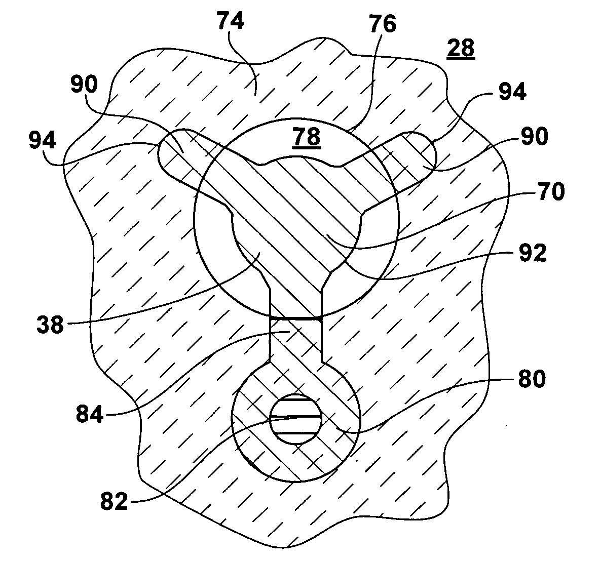
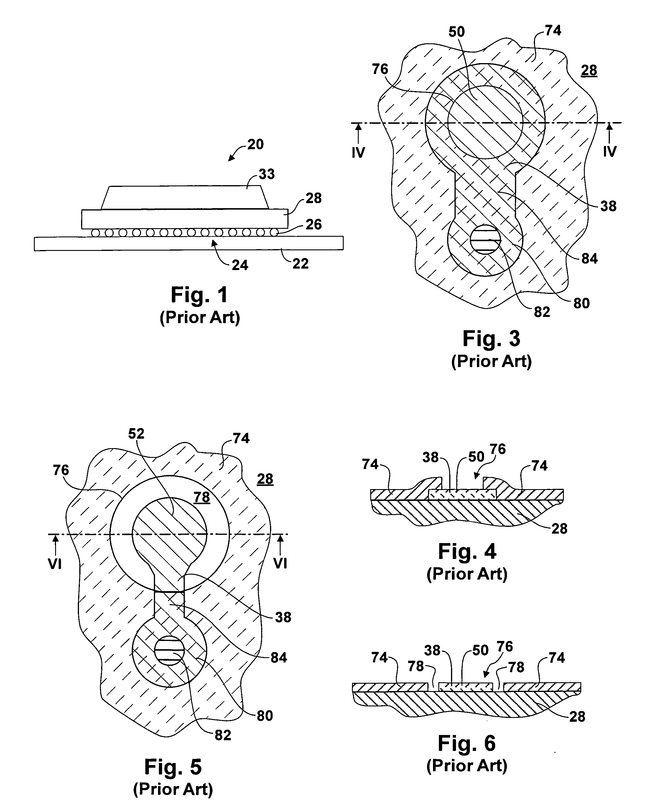
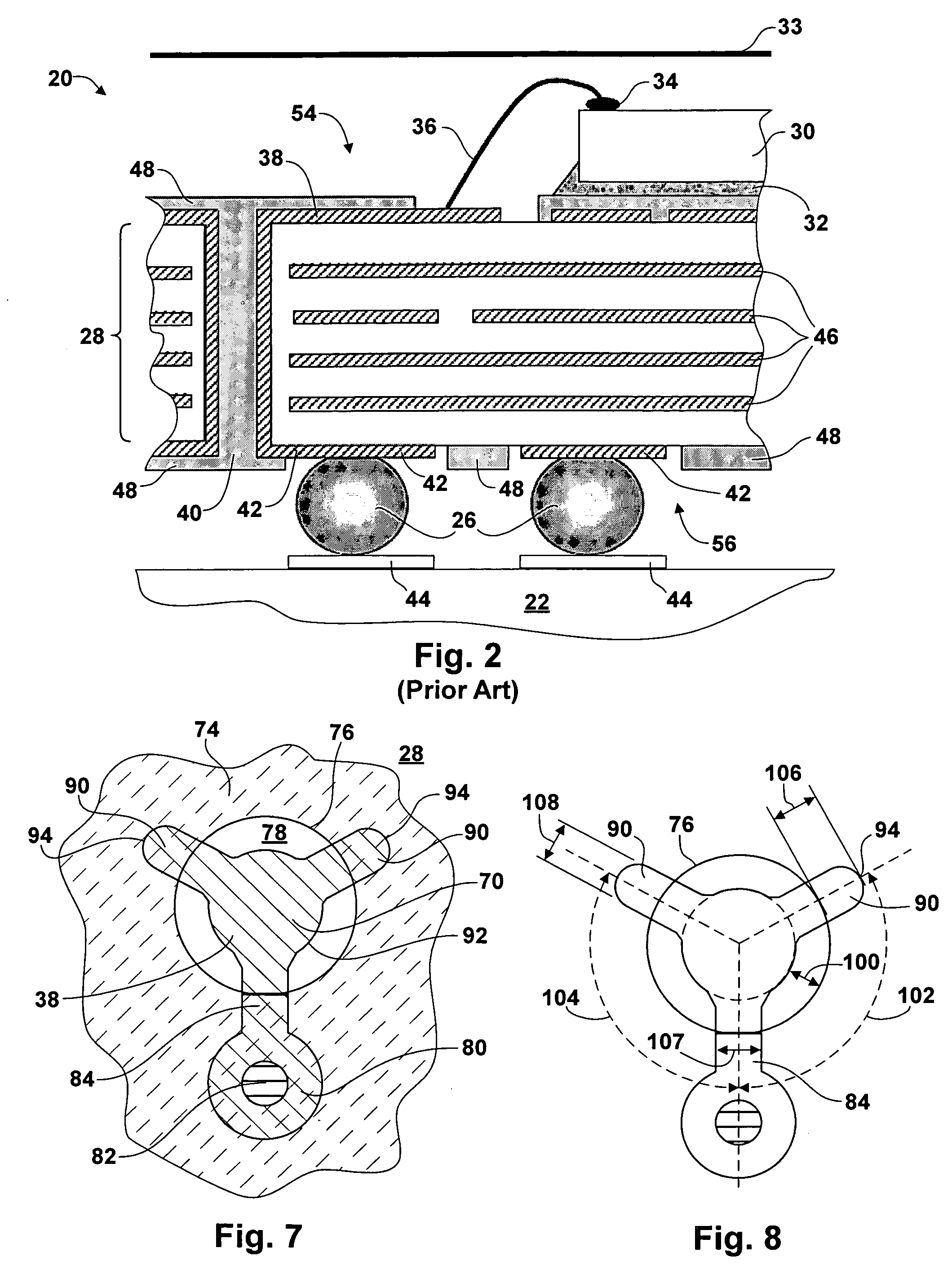
[0027] With reference now to the drawings, and in particular with reference to FIG. 2, there is depicted a partial section view of integrated circuit 20, which is shown in FIG. 1. As illustrated, integrated circuit 20 includes substrate 28 and integrated circuit die 30, which is mounted to substrate 28 by epoxy 32. Die 30 is covered and protected by cover 33 (which is also shown in FIG. 1). The surface of substrate 28 to which die 30 is mounted, may be referred to as “die mounting surface”54.

[0028] An electrical connection is made to die 30 at bond 34 using wire 36. Wire 36 carries signals, or power, to and from die 30 and conductor 38. Conductor 38 is adhered to, and is a part of, substrate 28. Integrated circuit signals pass along conductor 38, and, in the example illustrated, through via 40 to the opposite side of substrate 28 where substrate pads 42 are formed. The surface on which pads 42 are formed may be referred to as a “ball grid connection surface”56.

[0029] Solder balls ...


PUM


Abstract

A ball grid pad for connecting a ball grid array package to a printed circuit board includes a circular pad area adhered on a ball grid connection surface. A solder mask on the ball grid connection surface has an opening surrounding and spaced apart from the circular pad area. The ball pad includes an anchor trace on the ball grid connection surface wherein the ball pad conductor material extends radially from the edge of the circular pad area to a terminating point beyond the opening of the solder mask so that a portion of the anchor trace is covered by the solder mask. The ball grid connection surface may be an integrated circuit package substrate or a printed circuit board surface.

Description

BACKGROUND OF THE INVENTION [0001] 1. Field of the Invention [0002] The present invention relates generally to integrated circuits, and more specifically to designs for integrated circuits having packages and substrates using ball grid array packaging. Still more specifically, the present invention relates to an improved non-solder mask defined ball pad for an integrated circuit substrate and printed circuit board that uses a ball grid array. [0003] 2. Description of the Prior Art [0004] Many electronic products, such as computers, radios, and televisions, contain electronic components and integrated circuits that are mounted to printed circuit boards. To make a functional circuit, these electronic components are electrically connected to each other by metal traces that are printed like wires on the circuit board. Such “printed wires” lead from a connection point on one component to a connection point on another component. [0005] Electrical components are frequently mounted to the c...

Claims


Application Information

Patent Timeline
IPC IPC(8): H01L23/48
CPCH01L23/49816H05K1/114H05K3/3452H05K2201/09381H05K2201/0989H05K2201/099H05K2201/10734H01L2924/0002H01L2924/00
Inventor DAO, CHRISTINE HA
Owner STMICROELECTRONICS SRL
Why Eureka
Try Eureka