Semiconductor device connector, semiconductor device carrier, semiconductor device socket using the same and probe card

Inactive Publication Date: 2006-06-29
YAMAICHI ELECTRONICS
View PDF1 Cites 9 Cited by
  • Summary
  • Abstract
  • Description
  • Claims
  • Application Information

AI Technical Summary

Benefits of technology

[0023] By taking the above problems into account, the present invention provides a semiconductor device connector, a semiconductor device carrier capable of decreasing the variation of the degree of wear in the respective bump contact by restricting the inclination of the bump contact when the electrode section of the semiconductor device is brought into contact with the bump contacts, and a semiconductor device socket using the same and a probe card.

Problems solved by technology

In the prior art, however, since the contact pressure necessary for the contact of the electrode section in the semiconductor device with the bump contacts is properly determined with reference to the pressing force due to pressing member held by the semiconductor device carrier and the reactive force due to the elastic sheet disposed on the bottom of the electrode sheet when the semiconductor device carrier, the bump contacts of the electrode sheet in the semiconductor device socket and the electrode section of the semiconductor device are brought into contact with each other, there may be a risk of occurring such problems as illustrated in FIGS.
For example, when the tests are repeated a plurality of times, there may be a risk in that the electric connection of the bump contact touching with the extremity of the electrode section in the semiconductor device becomes unsafety.

Method used


Image

  • Semiconductor device connector, semiconductor device carrier, semiconductor device socket using the same and probe card
  • Semiconductor device connector, semiconductor device carrier, semiconductor device socket using the same and probe card
  • Semiconductor device connector, semiconductor device carrier, semiconductor device socket using the same and probe card

Examples


first embodiment

[0072] An embodiment according to the present invention will be described below with reference to the attached drawings.

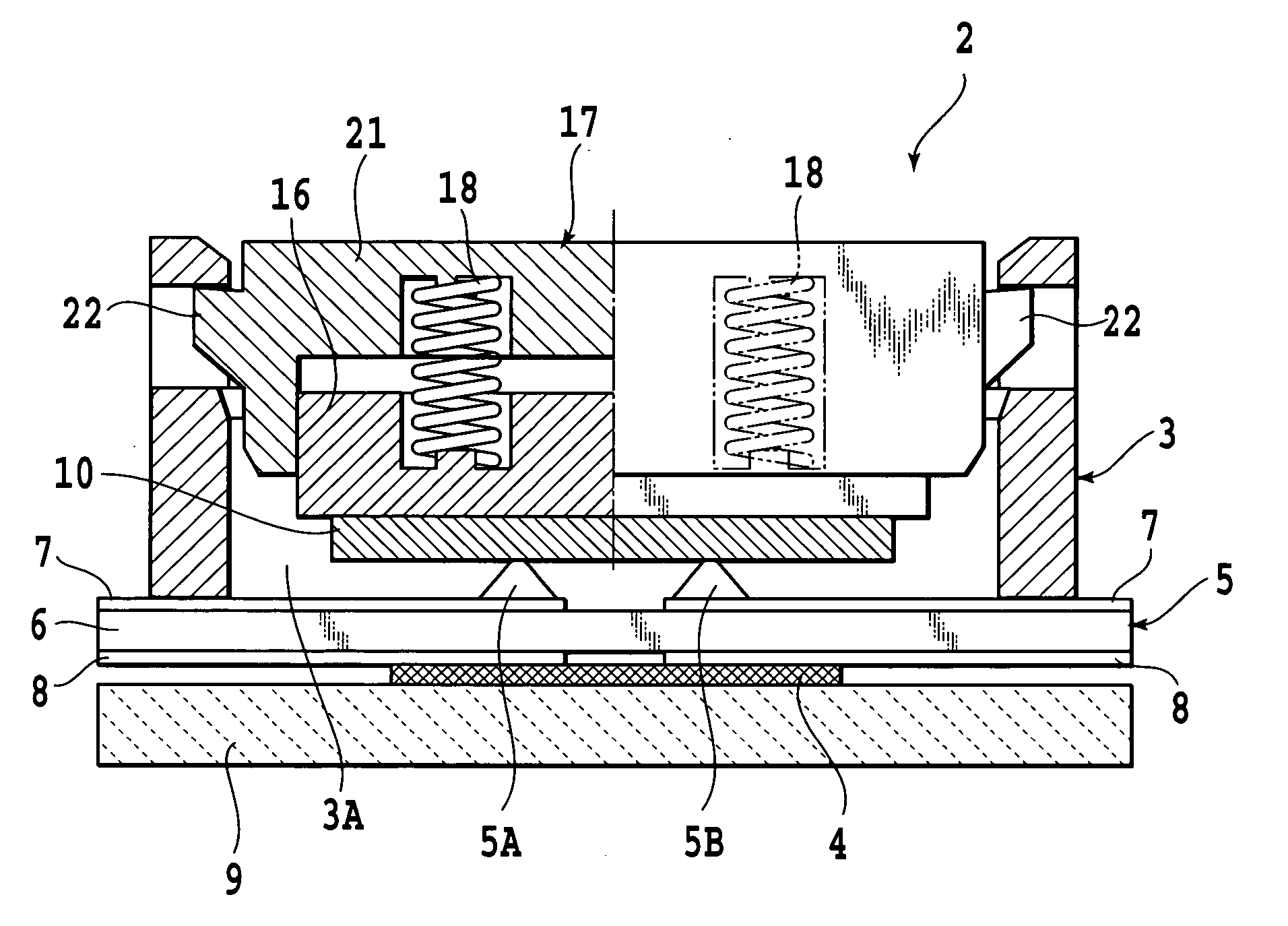
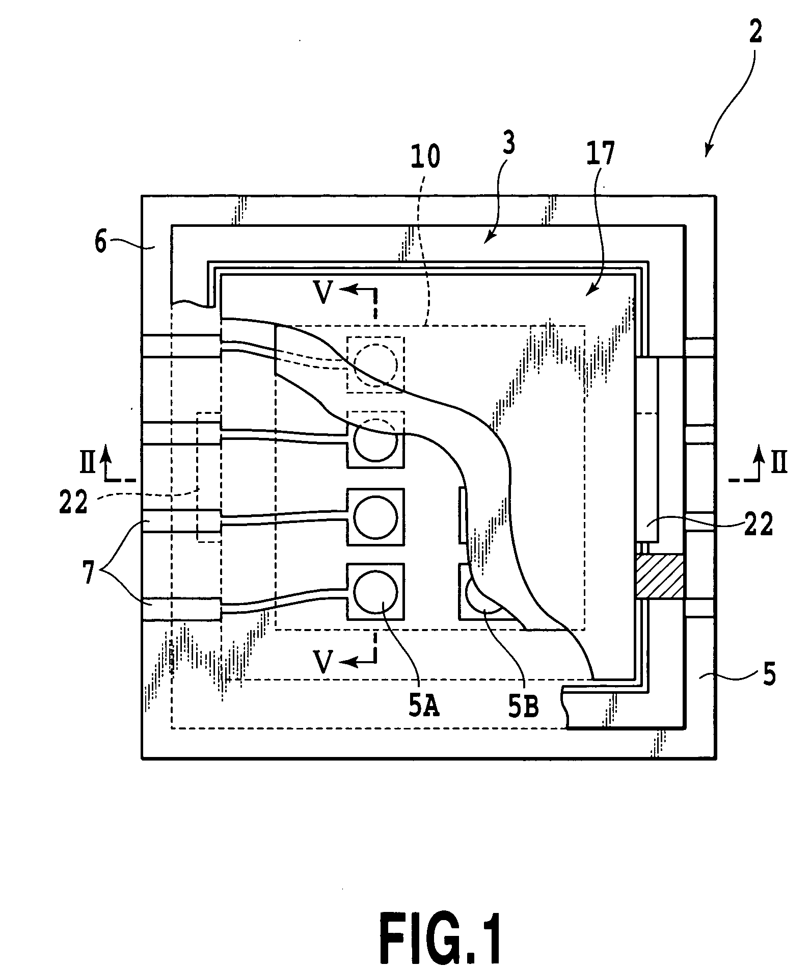
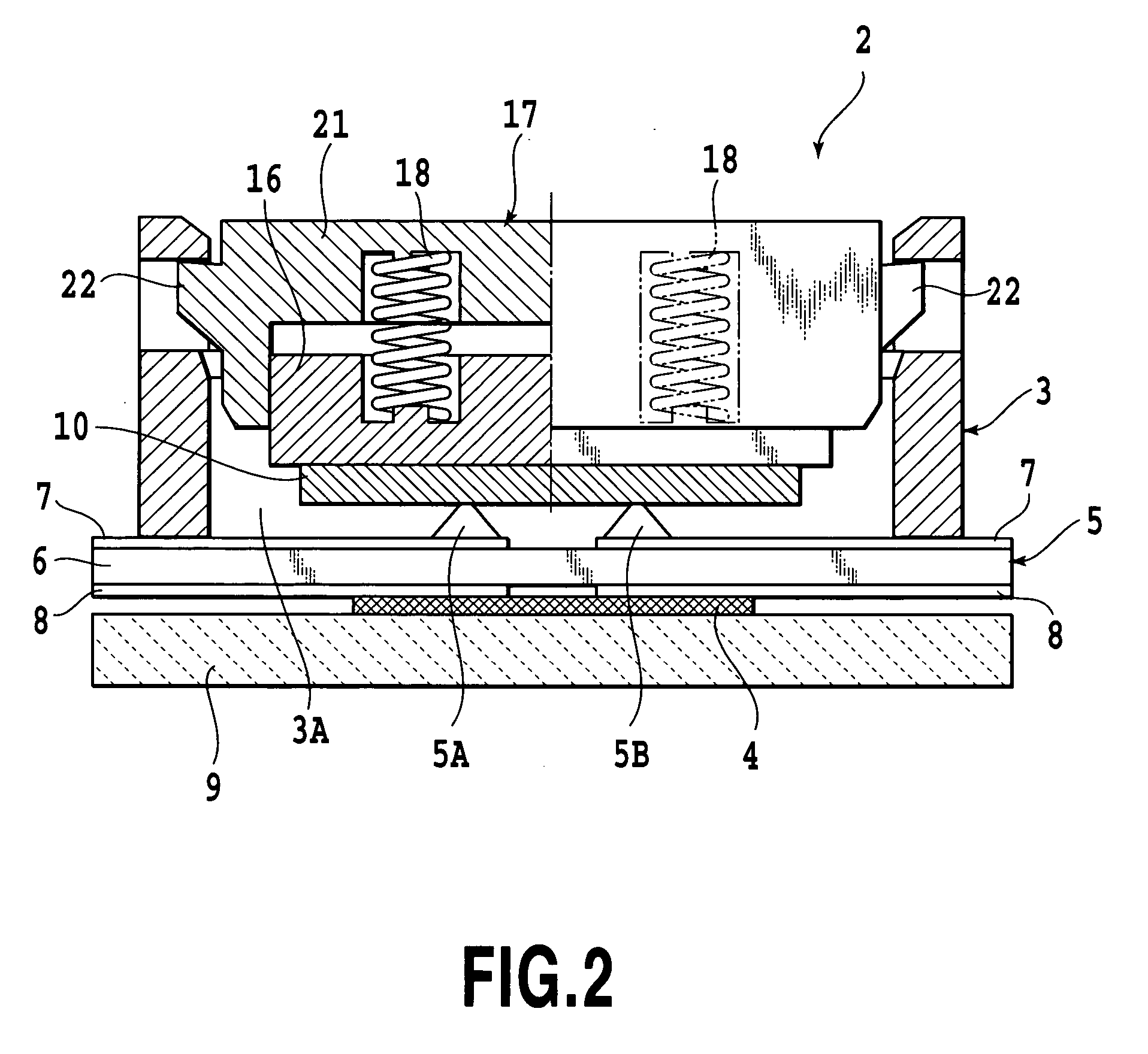
[0073]FIG. 1 is a partially plan view schematically illustrating one embodiment of a semiconductor device carrier in a semiconductor device socket according to the present invention; FIG. 2 is a partially sectional view of a main part of the semiconductor device carrier according to the present invention taken along a line II-II in FIG. 1; FIG. 3 is a partially sectional view schematically illustrating a total structure of the semiconductor device socket according to the present invention; FIG. 4 is a partially sectional view illustrating the operation of the embodiment of the semiconductor device socket according to the present invention shown in FIG. 3; FIG. 5 is a sectional view schematically illustrating a main part of the semiconductor device carrier taken along a line V-V in FIG. 1; FIG. 6 is a plan view of a front surface wiring of electric contacts in the ...

second embodiment

[0123] A second embodiment of the present invention is illustrated in FIGS. 20 to 24 wherein FIG. 20 is a sectional view schematically illustrating a main part of an electric contact structure in a semiconductor device carrier of a second embodiment; FIG. 21 is a plan view of the front surface wiring pattern of the electric contact structure in the semiconductor device carrier shown in FIG. 20; FIG. 22 is a vertical sectional view illustrating a contacting state of the semiconductor device and the bump contact; FIG. 23 is an enlarged view of part B in FIG. 22; and FIG. 24 is a plan view of collapsed shapes of tip ends of the bump contacts shown in FIG. 23;

[0124] The second embodiment is different from the first embodiment in that the conductor circuit provided on an insulation substrate for the electrode sheet is arranged solely on the front surface thereof and there are no rear surface wiring patterns.

[0125] That is, as illustrated, an electric contact structure 50 in the second ...


PUM


Abstract

A semiconductor device carrier comprising; a carrier housing having a housing portion for accommodating a semiconductor device; an electrode sheet disposed in the carrier housing, having a front surface wiring conductively arranged on a front surface of an insulation substrate, a rear surface wiring conductively arranged on a rear surface of the insulation substrate, a rear surface bump contact placement wiring, and a bump contact disposed in a contact placement portion and an elastic sheet disposed in the carrier housing to be in contact with the bottom of the electrode sheet; wherein a width of the rear surface bump contact placement wiring in correspondence to a bump contact to be in contact with an extreme electrode section of the semiconductor device is smaller than a width of the front surface bump contact placement wiring on which a bump contact to be in contact with the extreme electrode section is arranged.

Description

[0001] This application claims priority from Japanese Patent Applications Nos. 2004-374531 filed Dec. 24, 2004 and 2005-363829 filed Dec. 16, 2005, which are hereby incorporated by reference herein. BACKGROUND OF THE INVENTION [0002] 1. Field of the Invention [0003] The present invention relates to a semiconductor device connector, a semiconductor device carrier, a semiconductor device socket using the same and a probe card. [0004] 2. Description of the Related Art [0005] In the prior tart, semiconductor devices such as KGD (known good die) have been tested prior to being mounted to an electronic appliance or others. As a result, the semiconductor devices having any faults have been omitted. [0006] In such a test, the semiconductor devices are placed on a semiconductor device carrier that is then accommodated in a socket having a carrier housing portion fixed to a substrate such as a test board. Thereafter, the semiconductor devices are tested via the semiconductor device carrier an...

Claims


Application Information

Patent Timeline
IPC IPC(8): H01L23/12
CPCG01R1/0466H01R13/2464H01L2924/0002H01L2924/00
Inventor SUZUKI, TAKEYUKI
Owner YAMAICHI ELECTRONICS
Why Eureka
Try Eureka