Display device and display panel, pixel circuit and compensating method thereof

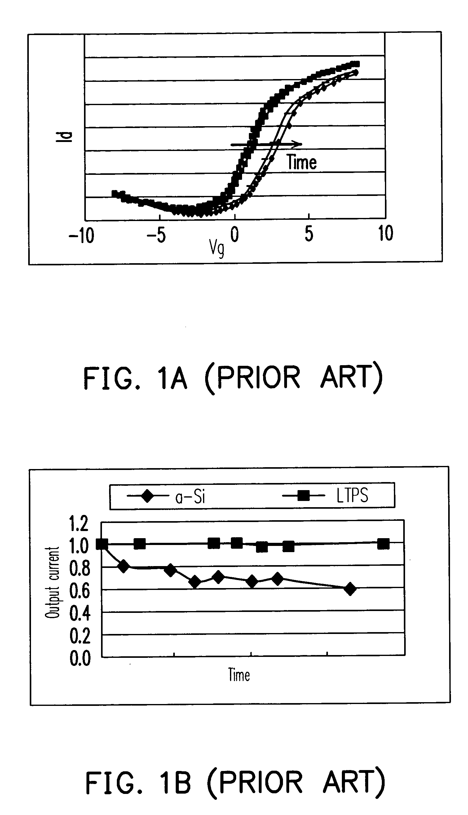
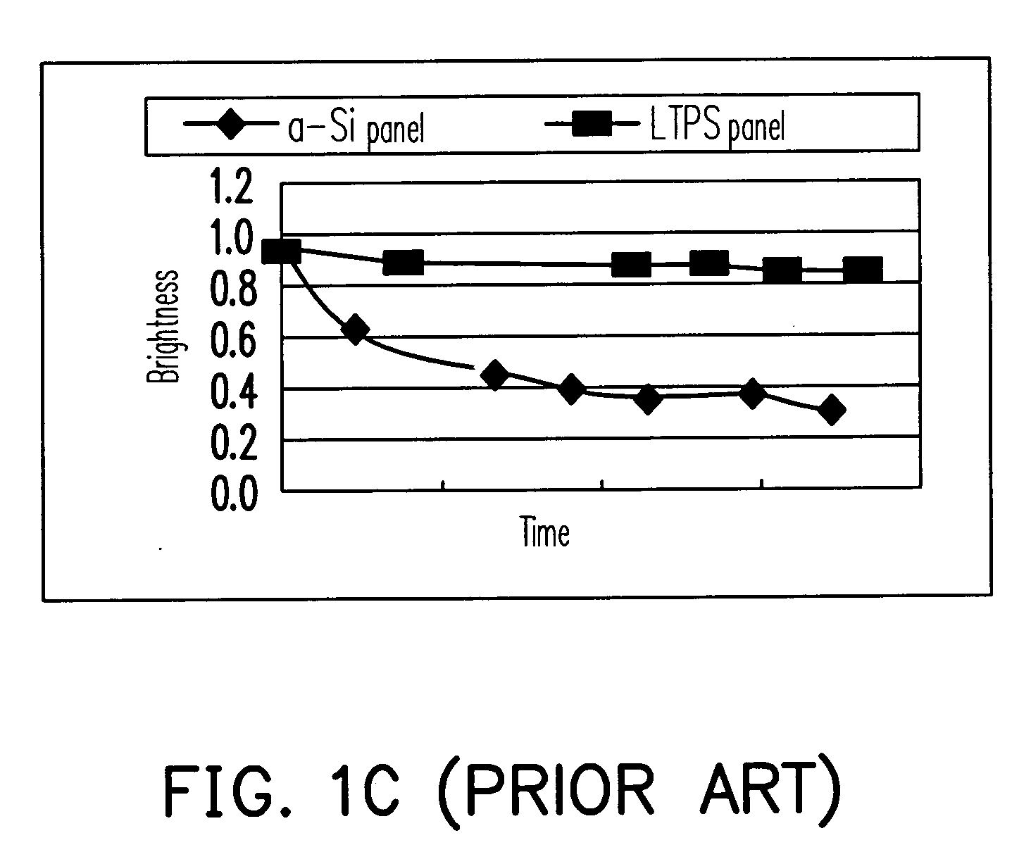
a display panel and display device technology, applied in the field of detection methods of display devices, can solve the problems of ltps tft technology cost, poor uniformity of tft-amoled display manufactured by ltps tft technology, and decay of brightness amoled display manufactured by a—si tft technology

Active Publication Date: 2006-06-29
AU OPTRONICS CORP
View PDF2 Cites 19 Cited by
  • Summary
  • Abstract
  • Description
  • Claims
  • Application Information

AI Technical Summary

Benefits of technology

[0013] Furthermore, the present invention is directed to a compensation method of a display device, suitable for amorphous silicon (a—Si TFT) AMOLED display, for stabilizing the output current of the pixel.
[0027] Accordingly, since the present invention provides a plurality of redundancy pixel cells for comparing the working current of the display pixel cells to the standard reference current, the shift of the working current of the display pixel cells may be readily detected. Moreover, the present invention also provides a programmable voltage generator. Thus, when the shift of the working current of each display pixel cell is detected, the timing controller of the present invention may adjust the programmable voltage generator to generate a voltage level of the data to compensate the display pixel cell. Thus, the brightness of the frame may be steady even after a period of time.

Problems solved by technology

As shown in table 1, it is noted that the uniformity of the TFT-AMOLED display manufactured by the LTPS TFT technology is not good, and the cost of LTPS TFT technology is high due to comparatively larger number of masking processes.
However, the brightness AMOLED display manufactured by a—Si TFT technology decays after working for a period of time since the output current stability of a—Si TFT technology is poor.

Method used


Image

  • Display device and display panel, pixel circuit and compensating method thereof
  • Display device and display panel, pixel circuit and compensating method thereof
  • Display device and display panel, pixel circuit and compensating method thereof

Examples


Embodiment Construction

[0038] The present invention now will be described more fully hereinafter with reference to the accompanying drawings, in which embodiments of the invention are shown. This invention may, however, be embodied in many different forms and should not be construed as limited to the embodiments set forth herein; rather, these embodiments are provided so that this disclosure will be thorough and complete, and will fully convey the scope of the invention to those skilled in the art. Like numbers refer to like elements throughout.

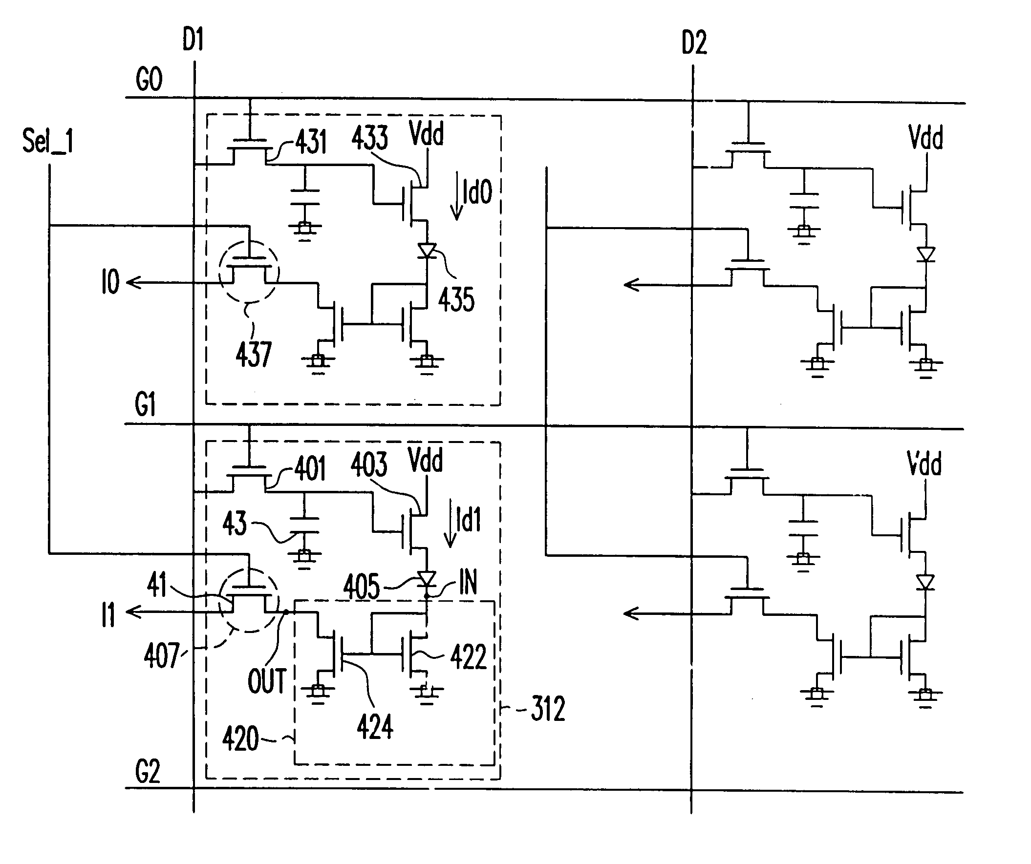
[0039]FIG. 2A is a schematic circuit block diagram of a display device according to one embodiment of the present invention. Referring to FIG. 2A, the display device of the present invention may comprise a display panel 310 connected to a gate driver circuit 321 and a source driver circuit 323 via scan lines G1 to Gm-1 and data lines D1 to Dn respectively. In addition, the present invention may further comprise a timing control circuit 330 adopted for controlling ...


PUM


Abstract

A display device including a timing control circuit, a programmable voltage generator, a gate driver, a source driver circuit and a display panel is provided. The display panel includes a plurality of redundancy pixel cells and display pixel cells. The redundancy pixel cells and display pixel cells may include a—Si TFT and organic light emitting diode. The redundancy pixel cells and display pixel cells may be turned on by the gate driver circuit, and the working current of each display pixel cell may be compared with that of the corresponding redundancy pixel cell. Then timing control circuit may control the programmable voltage generator to generate applicable voltage of data to the source driver circuit to compensate the shift of the working current of the display pixel cells after working a period of time according to the comparison result.

Description

CROSS-REFERENCE TO RELATED APPLICATION [0001] This application claims the priority benefit of Taiwan application serial no. 93140413, filed on Dec. 24, 2005. All disclosure of the Taiwan application is incorporated herein by reference. BACKGROUND OF THE INVENTION [0002] 1. Field of the Invention [0003] The present invention relates to a detection method of a display device. More particularly, the present invention relates to detection method of a display device including pixel devices constructed by organic light emitting diode. [0004] 2. Description of Related Art [0005] With the rapid advancement of multimedia technology, semiconductor component and display device technology have progressively developed. In the conventional flat display device, since thin film transistor active matrix organic light emitting diode (TFT-AMOLED) display has the advantages of free of view-angle dependence, low cost, high response speed (about hundreds of times compared to liquid crystal display device...

Claims


Application Information

Patent Timeline
Patent Type & Authority Applications(United States)
IPC IPC(8): G09G3/30
CPCG09G3/3241G09G2300/0417G09G2300/0842G09G2300/0861G09G2300/0866G09G2320/029G09G2320/043
Inventor LEE, I-SHU
Owner AU OPTRONICS CORP
Why Eureka
Try Eureka