Method of fabricating and integrated circuit to improve soft error performance

a technology of integrated circuits and manufacturing methods, applied in the field of manufacturing integrated circuits, can solve the problems of soft error reliability, affecting logic state, and increasing difficulty in complex system on-chip (soc) design, so as to reduce soft error risk and reduce linear energy transfer

Active Publication Date: 2006-07-06
TEXAS INSTR INC
View PDF3 Cites 11 Cited by
  • Summary
  • Abstract
  • Description
  • Claims
  • Application Information

AI Technical Summary

Benefits of technology

[0007] To address the above-discussed deficiencies of the prior art, the present invention provides, in one embodiment, a method of designing an integrated circuit. In this particular embodiment, the method comprises reducing soft error risk in an integrated circuit by locating a structure relative to a node of the integrated circuit to reduce a linear energy transfer associated with a sub-atomic particle into the node, such that the linear energy transfer does not exceed a threshold value associated with the integrated circuit.
[0008] In another embodiment, the present invention provides a method for fabricating an integrated circuit. This particular embodiment comprises configuring an optimized integrated circuit design by selectively locating interconnect structures relative to source/drain regions to reduce a linear energy transfer associated with sub-atomic particles into the source/drain regions...

Problems solved by technology

As the size of transistors descends further into the deep submicron range, integrated circuits are becoming increasingly susceptible to operational disturbances caused by fluctuations in the surrounding environment.
By imparting unwanted charge into random nodes of an integrated circuit, these particle strikes can either toggle the states of storage elements or cause poorly-timed transient glitches that disrupt the latching of combinational results.
However, with ever shrinking geometries and higher-density circuits, the issue of soft errors and reliability in complex System on Chip (SoC) design is set to become an increasingly challenging issue for the industry as a whole.
For example, high energy particles, such as cosmic radiation or alpha particles emanating from packaging materials can interfere with charges held within sensitive nodes in the circuit, thereby affecting the logic state.
These soft errors, which are also known as single-event upsets, generally affect storage elements, such as memo...

Method used


Image

  • Method of fabricating and integrated circuit to improve soft error performance
  • Method of fabricating and integrated circuit to improve soft error performance
  • Method of fabricating and integrated circuit to improve soft error performance

Examples


Embodiment Construction

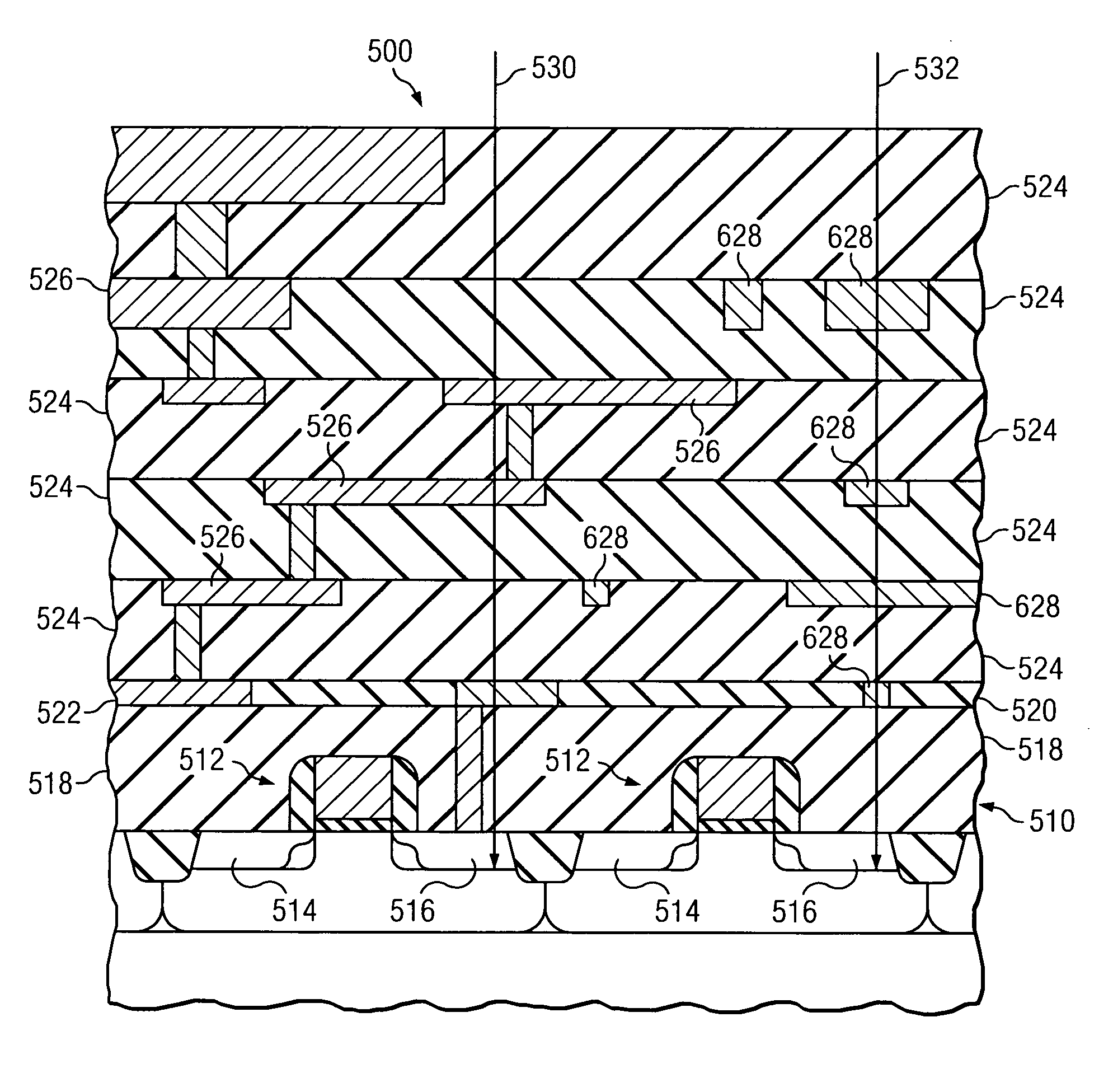
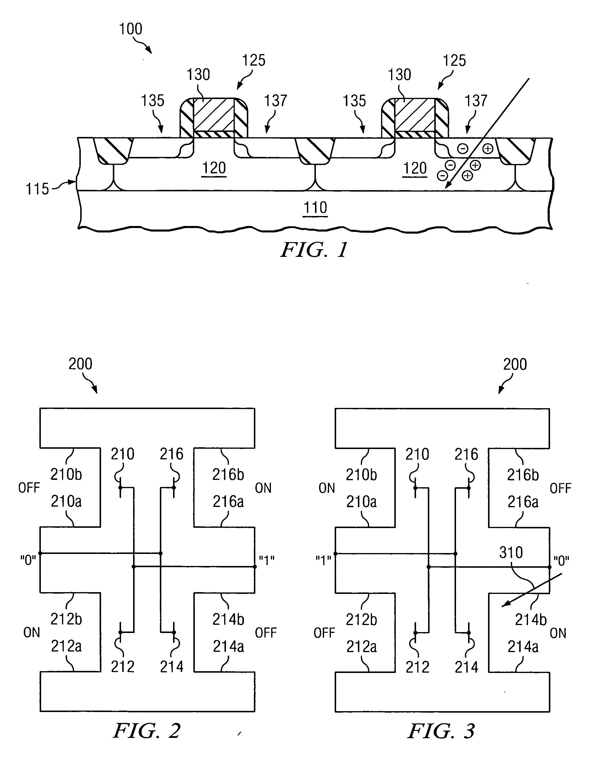
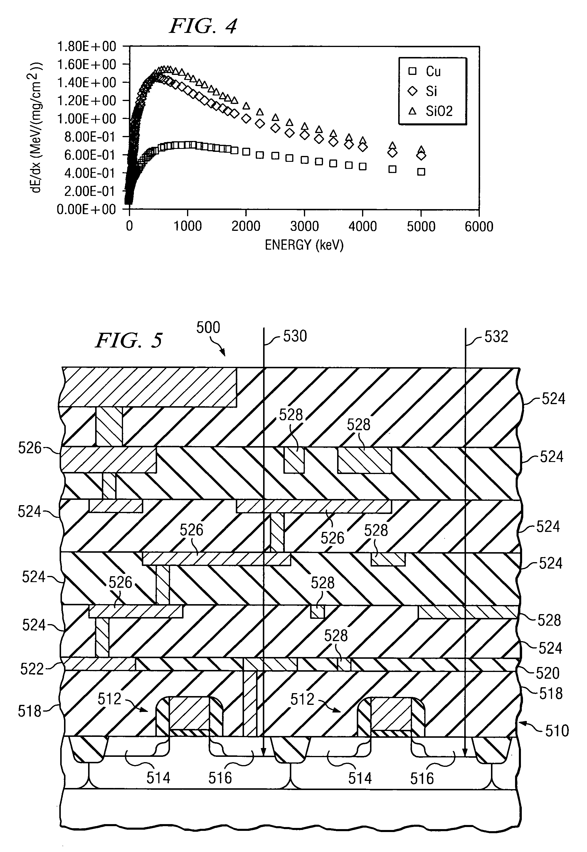
[0018] The present invention recognizes the problems associated with soft errors that occur when sub-atomic particles encounter nodes within an integrated circuit and impart energy or a charge sufficient to change the logic state of one or more of the nodes. This can and does happen in memory circuits, such as static random access memory (SRAM) circuits and is occurring with more frequency as device sizes have reached well into the submicron range. The present invention presents a unique solution in solving this problem and one that does not suffer from the disadvantages associated with the prior art processes discussed above. The present invention comprises reducing soft error risk in an integrated circuit by locating a structure, such as a layer of material, an interconnect structure, a capacitor, inductor or resistor, relative to a node of the integrated circuit to reduce a linear energy transfer, which is associated with sub-atomic particles, into the node. The structure is loca...


PUM


Abstract

The present invention provides, in one aspect, a method of designing an integrated circuit 500. In this particular aspect, the method comprises reducing soft error risk in an integrated circuit 500 by locating a structure 526, 528 relative to a node 516 of the integrated circuit 500 to reduce a linear energy transfer associated with a sub-atomic particle 530, 532 into the node 516, such that the linear energy transfer does not exceed a threshold value associated with the integrated circuit 500.

Description

TECHNICAL FIELD OF THE INVENTION [0001] The present invention is directed in general to a method of fabricating an integrated circuit and, more specifically, to a method of improving soft error performance in an integrated circuit through selective layer placement. BACKGROUND [0002] As the size of transistors descends further into the deep submicron range, integrated circuits are becoming increasingly susceptible to operational disturbances caused by fluctuations in the surrounding environment. These fluctuations are often referred to as “soft errors.” It is believed that these soft errors are primarily produced by energetic particle strikes. By imparting unwanted charge into random nodes of an integrated circuit, these particle strikes can either toggle the states of storage elements or cause poorly-timed transient glitches that disrupt the latching of combinational results. In older technologies, this was not a significant problem, because the capacitances of the larger devices an...

Claims


Application Information

Patent Timeline
IPC IPC(8): G06F17/50
CPCG06F17/5045H01L27/11G06F30/30H10B10/00
Inventor ZHU, XIAOWEIBAUMANN, ROBERT C.
Owner TEXAS INSTR INC
Why Eureka
Try Eureka