High mobility plane finfet with equal drive strength

Inactive Publication Date: 2006-07-13
IBM CORP
View PDF8 Cites 25 Cited by
  • Summary
  • Abstract
  • Description
  • Claims
  • Application Information

AI Technical Summary

Benefits of technology

[0006] This disclosure presents, in one embodiment, a method of forming an integrated circuit structure having a first-type (e.g., N-type) fin-type field effect transistor (FinFET) and a second-type (e.g., P-type) FinFET above a buried oxide (BOX) layer. This method begins by forming the BOX layer on a first-type wafer and bonding the BOX layer to a second-type wafer to join the first-type wafer to the second-type wafer to form a structure having the first-type layer and the second-type layer separated by the BOX layer. The method removes a

Problems solved by technology

Conventional FinFETs that utilize different types of transistors (e.g., N-type and P-type FinFETs)

Method used


Image

  • High mobility plane finfet with equal drive strength
  • High mobility plane finfet with equal drive strength
  • High mobility plane finfet with equal drive strength

Examples


Example

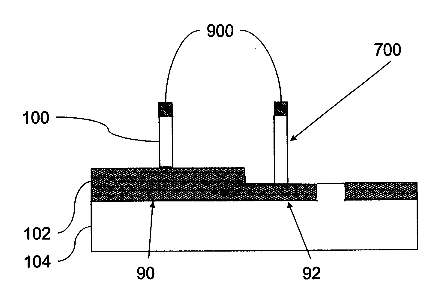
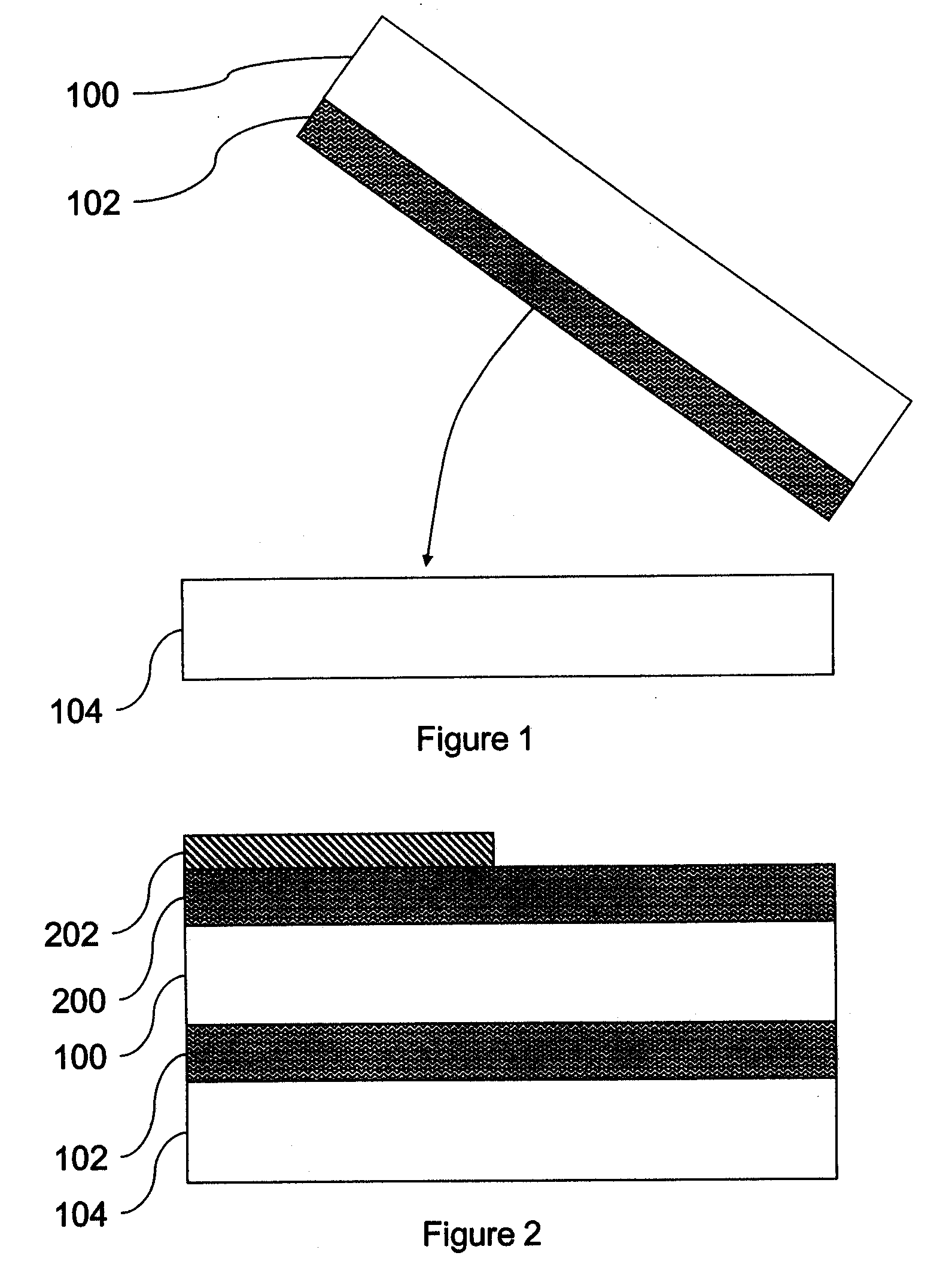
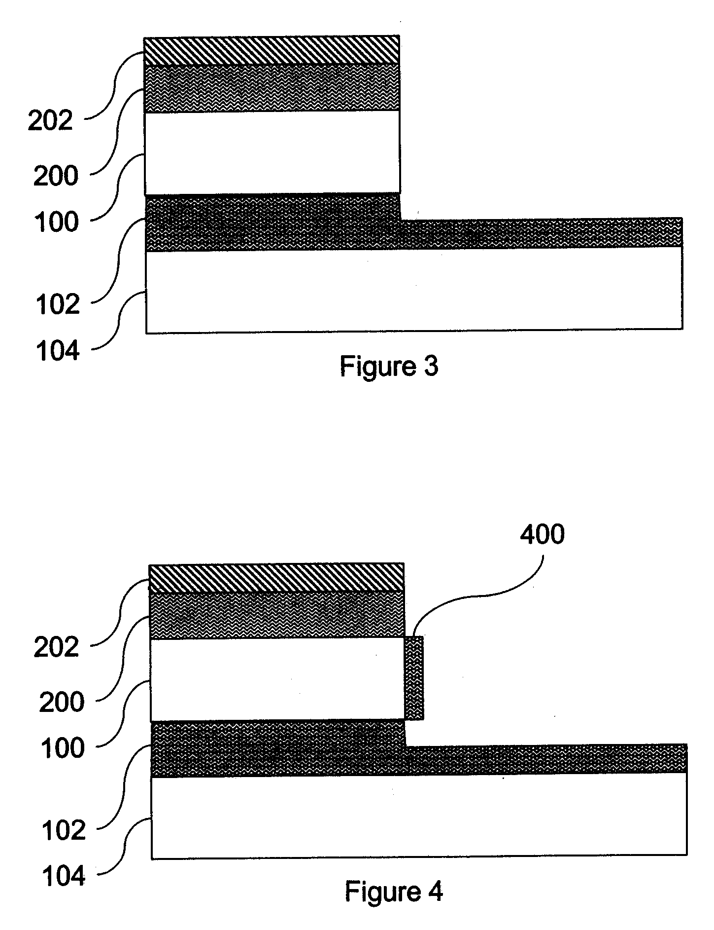
[0029] The present invention and the various features and advantageous details thereof are explained more fully with reference to the nonlimiting embodiments that are illustrated in the accompanying drawings and detailed in the following description. It should be noted that the features illustrated in the drawings are not necessarily drawn to scale. Descriptions of well-known components and processing techniques are omitted so as to not unnecessarily obscure the present invention. The examples used herein are intended merely to facilitate an understanding of ways in which the invention may be practiced and to further enable those of skill in the art to practice the invention. Accordingly, the examples should not be construed as limiting the scope of the invention.

[0030] As shown in FIG. 1, a BOX layer 102 (such as SiO2) is formed on a first-type wafer 100. The BOX layer 102 comprises the bonding agent (adhesive) that bonds the first-type wafer 100 to a second-type wafer 104. This f...


PUM


Abstract

An integrated circuit structure has a buried oxide (BOX) layer above a substrate, and a first-type fin-type field effect transistor (FinFET) and a second-type FinFET above the BOX layer. The second region of the BOX layer includes a seed opening to the substrate. The top of the first-type FinFET and the second-type FinFET are planar with each other. A first region of the BOX layer below the first FinFET fin is thicker above the substrate when compared to a second region of the BOX layer below the second FinFET fin. Also, the second FinFET fin is taller than the first FinFET fin. The height difference between the first fin and the second fin permits the first-type FinFET to have the same drive strength as the second-type FinFET.

Description

BACKGROUND OF THE INVENTION [0001] 1. Field of the Invention [0002] The invention generally relates to an integrated circuit structure having a first-type (e.g., N-type) fin-type field effect transistor (FinFET) and a second-type (e.g., P-type) FinFET above a buried oxide (BOX) layer, where the second FinFET fin is taller than the first FinFET fin and where the height difference between the first fin and the second fin permits the first-type FinFET to have the same drive strength as the second-type FinFET. [0003] 2. Description of the Related Art [0004] As transistor design is improved and evolves, the number of different types of transistors continues to increase. For example, one type of transistor that uses a fin-shaped channel region covered with a gate conductor, with the outer portions of the fin being used as source / drain regions is referred to as a fin-type field effect transistor (FinFET). One such FinFET is disclosed in U.S. Pat. No. 6,413,802 to Hu et al. (hereinafter “Hu...

Claims


Application Information

Patent Timeline
IPC IPC(8): H01L29/772H01L21/336H01L21/8238
CPCH01L21/84H01L27/1203H01L29/66795H01L29/785H01L29/78603
Inventor ANDERSON, BRENT A.NOWAK, EDWARD J.
Owner IBM CORP
Why Eureka
Try Eureka