Electrostatic discharge protection for embedded components

a technology of embedded components and electrostatic discharge protection, which is applied in the direction of circuit electrostatic discharge protection, printed resistor incorporation, overvoltage protection resistors, etc., can solve the problem of potentially reducing the overall size of the pcb, and achieve the effect of reducing costs

Inactive Publication Date: 2006-07-13
LITTELFUSE INC
View PDF50 Cites 64 Cited by
  • Summary
  • Abstract
  • Description
  • Claims
  • Application Information

AI Technical Summary

Benefits of technology

[0015] In another primary embodiment of the present invention, the VVM is applied as a layer to a conductive foil to form an active substrate or active laminate. The resulting active laminate may be partially cured and applied to a supporting substrate, such as a rigid PCB. In the present invention, the VVM layer is coated or applied to a conductive, e.g., copper, layer to produce the active substrate or laminate. The active substrate is used in combination with embedded electrical components in many different ways as shown in detail below. In an embodiment, the electrical components are also applied as a layer, e.g., laminated to the exposed side of the VVM layer of the active laminate. The active substrate conveniently replaces an otherwise necessary insulative layer. The active substrate also extends in multiple directions so that the substrate can protect multiple electrical components.
[0016] The active substrate provides each of the same benefits as the embedded VVM embodiments, such as conserved board space, reduced cost, etc. The active substrate is also an embedded VVM application, in which the VVM layer doubles as a normal voltage state insulating substrate.
[0017] The VVM layer can be placed in a parallel electrical arrangement with the embedded electrical component(s). The VVM layer may also form gaps in the X-Y or Z directional arrangements described above. The PCB employing the VVM layer and active substrate may include one or more vias that enable energy to be shunted to different conductive layers within the PCB. The PCB may include a plurality of VVM or active substrate layers, combine the VVM layer with one or more insulative substrates and protect a variety of different types of embedded electrical components.

Problems solved by technology

The electrical component film and the VVM layer are imbedded within the PCB, saving valuable space on the surface of the PCB and potentially reducing the overall size needed for the PCB.

Method used


Image

  • Electrostatic discharge protection for embedded components
  • Electrostatic discharge protection for embedded components
  • Electrostatic discharge protection for embedded components

Examples


Embodiment Construction

Overview

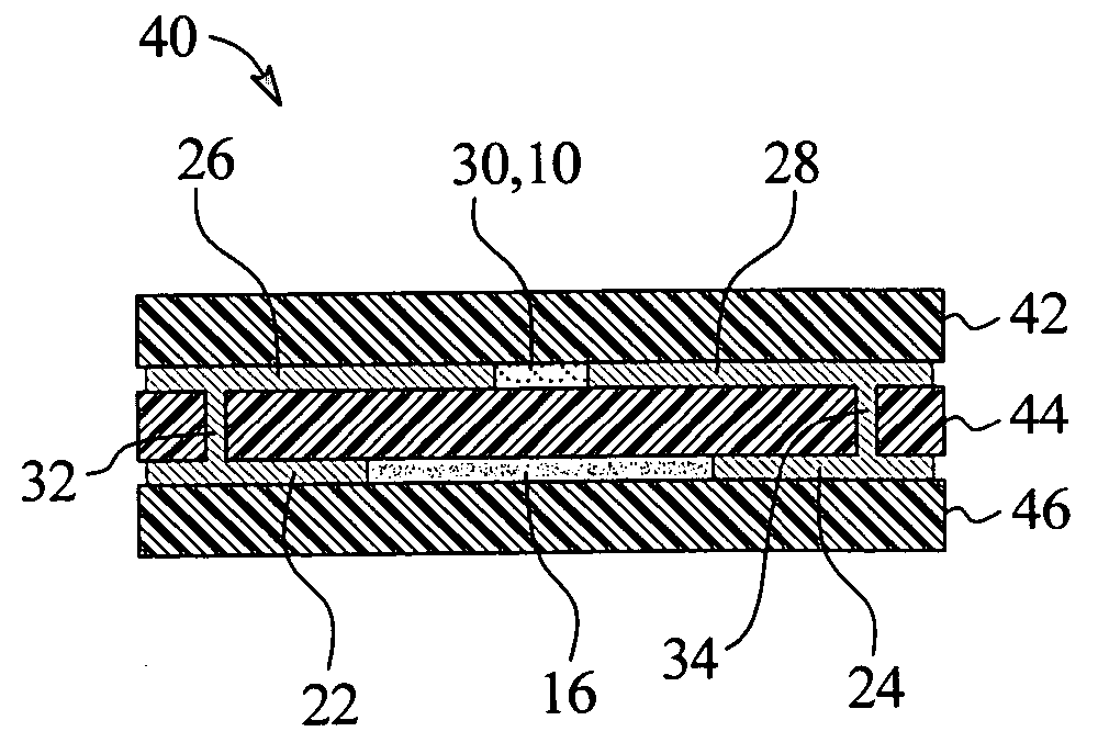
[0034] In one primary embodiment of the present invention, electrical components such as resistors and capacitors are embedded with voltage variable material (“VVM”) in a printed circuit board (“PCB”), such as a multilayer PCB. In one implementation, the electrical components are provided as a film that is laminated onto an insulative substrate of the PCB or between two such substrates. The VVM is also laminated to an insulative substrate, such as an opposite side of the substrate from which the electrical component film is laminated. The combination of the insulative substrate(s), component film and VVM can be provided as a device or as a PCB capable of receiving circuit traces, surface-mounted components, through-hole components and other items.

[0035] The embedded components and VVM reduces the overall size and cost of a resulting device or PCB. The embedded components and VVM also frees space on the outsides, e.g., top and bottom sides, of the PCB and improves signal in...


PUM


Abstract

An improved electrical circuit that includes an embedded electrical component and an embedded voltage variable material (“VVM”) is provided. In one embodiment, the embedded VVM is provided as a voltage variable substrate, which is used in combination with an embedded electrical component, such as an embedded resistive material or an embedded capacitive material.

Description

CROSS-REFERENCE TO RELATED APPLICATIONS [0001] This application is related to the following commonly-owned co-pending patent applications: U.S. patent application Ser. No. 10 / 958,442, filed Oct. 5, 2004, entitled “Direct Application Variable Material, Devices Employing Same And Methods Of Manufacturing Such Devices,” which claims priority as a continuation-in-part to U.S. patent application Ser. No. 10 / 746,020, filed Dec. 23, 2003, entitled “Direct Application Voltage Variable Material, Components Thereof And Devices Employing Same,” which claims priority as a continuation-in-part to U.S. patent application Ser. No. 10 / 410,393, filed Apr. 8, 2003, entitled “Voltage Variable Material For Direct Application And Devices Employing Same,” which claims priority of U.S. Provisional Patent Application No. 60 / 370,975, filed Apr. 8, 2002, entitled “Voltage Variable Material For Direct Application And Devices Employing Same,” and U.S. patent application Ser. No. 09 / 976,964, filed Oct. 11, 2001...

Claims


Application Information

Patent Timeline
Patent Type & Authority Applications(United States)
IPC IPC(8): H01C3/06
CPCH01C7/003H01C7/12H05K1/0259H05K1/0373H05K1/16H05K1/162H05K1/165H05K1/167H05K3/4069H05K3/4626H05K3/4652H05K3/4655H05K3/4688H05K2201/0187H05K2201/0215H05K2201/0738H05K2201/09509
Inventor MAERCKLEIN, NATHANIELVYAS, TUSHARPACHLA, TIMOTHYWHITNEY, STEPHEN
Owner LITTELFUSE INC
Why Eureka
Try Eureka