
Eureka
For R&D, Eureka makes reading and utilizing patents & technical documents easy.
Eureka AIR
Designed for self-driven R&D workflows. Generate viable solutions, solve complex R&D challenges, empower your innovation with AI.

Eureka Materials
Designed for material experts only. Revolutionize your material R&D, from search, analyze, to developing new materials.

TechResearch
Generate reliable direction feasibility study reports for your R&D in just a few steps.

TechSeek
Discover and master advanced knowledge NOW. Basics, ideas, possibilities, all at once.

TechMind
As an expert in R&D Theories, TechMind can generates customized viable solutions instantly.

TechRisk
Analyze your overall solution with one click, know your potential R&D risks in advance.

TechMonitor
Get weekly tech updates, stay abreast of the latest tech innovations and key insights.
Coupling system between dielectric optical guides and planar photonic crystal guides
- Summary
- Abstract
- Description
- Claims
- Application Information
AI Technical Summary
Benefits of technology
Problems solved by technology
Method used
Image

Examples
Embodiment Construction
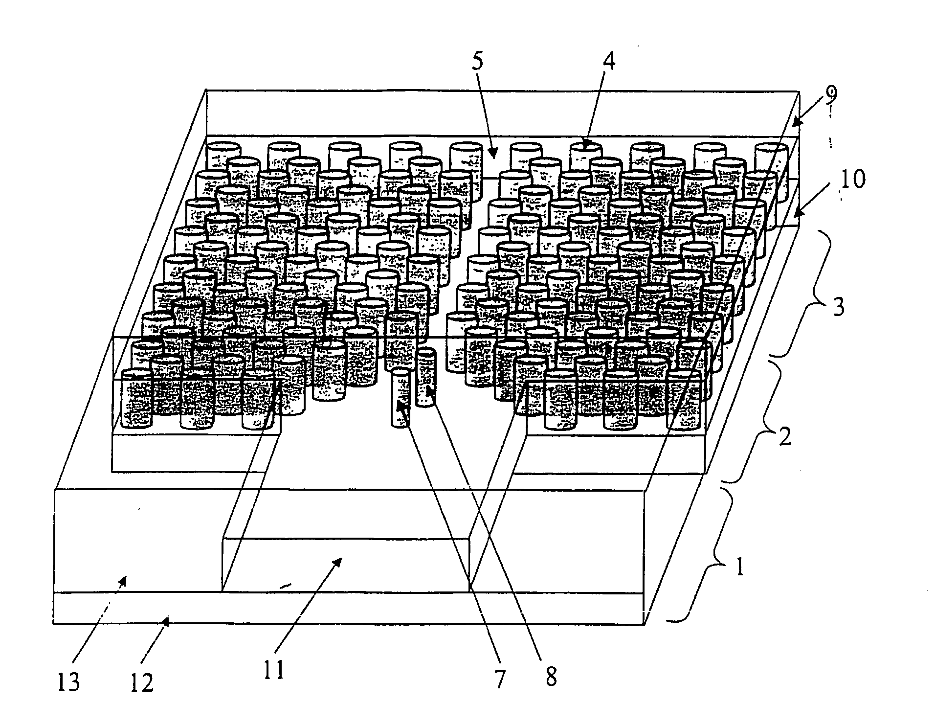
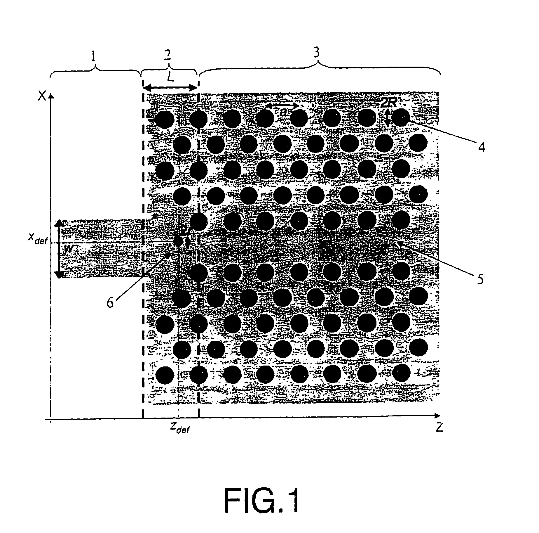
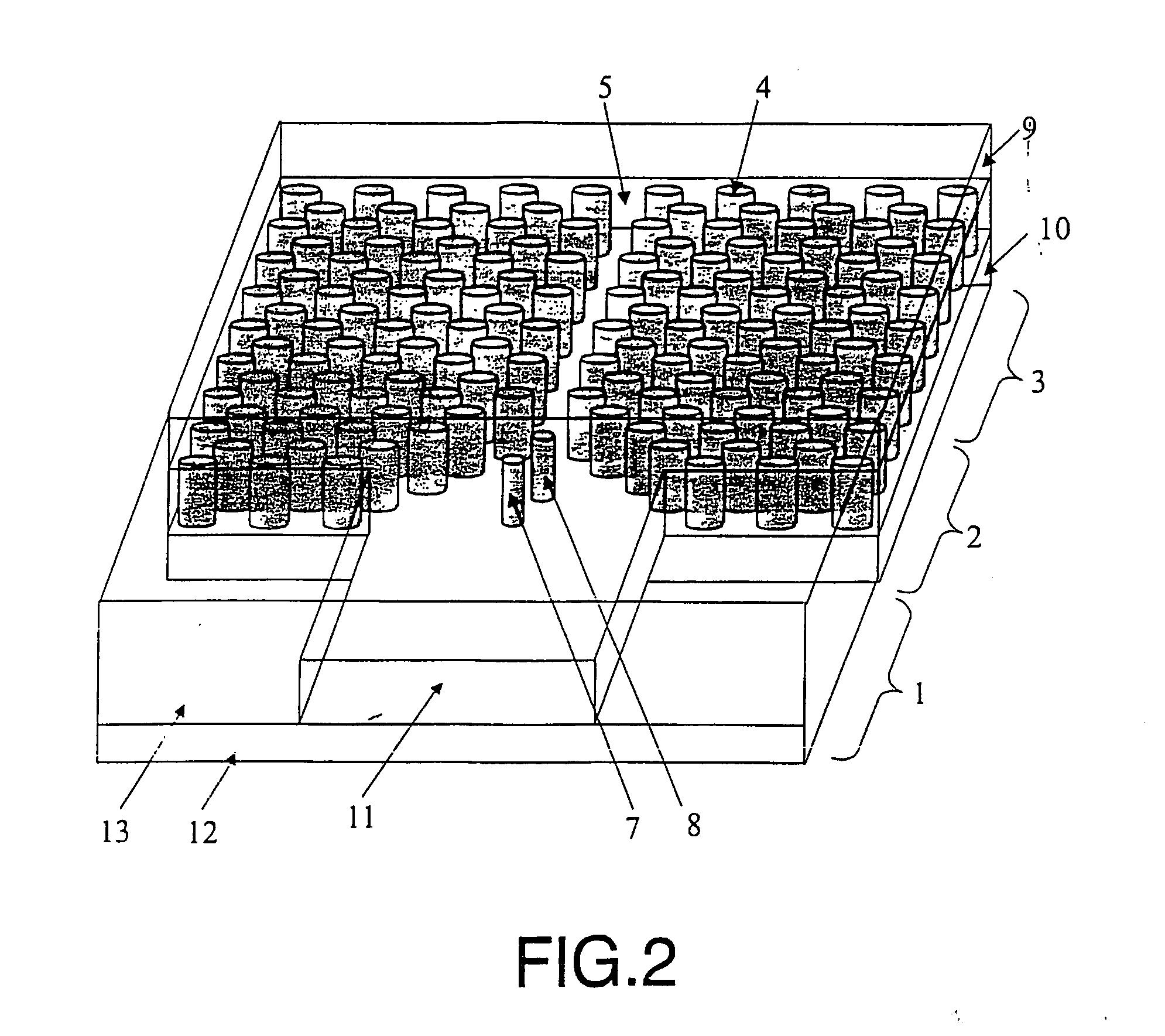
[0010] The purpose of this invention is a coupling technique based on the introduction of one or more point defects of specific characteristics into the aforementioned coupling structure. The introduction of the defects acts as an impedance adaptor thereby optimising the coupling efficiency between the dielectric guide and the photonic crystal guide.
[0011] The number of defects as well as the characteristics of each one of them will depend both on the characteristics of the dielectric and photonic crystal guides and on the characteristics of the coupling structure used to adapt the widths between both guides. This technique considerably improves coupling efficiency in a wide range of frequencies with regard to the structure without defects and, moreover, it is useful for both introducing and extracting light from devices made from planar photonic crystals. Furthermore, this technique optimises coupling not only to standard photonic crystal guides but also to other kinds of photonic...
PUM
 Abstract
Description
Claims
Application Information
 - R&D Engineer
- R&D Manager
- IP Professional
- Industry Leading Data Capabilities
- Powerful AI technology
- Patent DNA Extraction
Browse by: Latest US Patents, China's latest patents, Technical Efficacy Thesaurus, Application Domain, Technology Topic, Popular Technical Reports.
© 2024 PatSnap. All rights reserved.Legal|Privacy policy|Modern Slavery Act Transparency Statement|Sitemap|About US| Contact US: help@patsnap.com