Light emitting device with an incorporated optical wavelight layer

a light emitting device and optical wavelight technology, applied in the direction of discharge tube/lamp details, organic semiconductor devices, discharge tubes luminescnet screens, etc., can solve the problems of large amount of light generated at the light-emitting layers, loss in the display system, and ineffective use of display lights, etc., to achieve good efficiency, improve light extraction ratio, and high picture quality

Active Publication Date: 2006-04-18
SAMSUNG DISPLAY CO LTD
View PDF8 Cites 55 Cited by
  • Summary
  • Abstract
  • Description
  • Claims
  • Application Information

AI Technical Summary

Benefits of technology

[0013]In short, the light guided in parallel to the substrate therefore regarded as light loss in the conventional technologies is guided to the tilted reflective surface in a good efficiency and the light extracting ratio is improved. In this case, since the optical waveguide layer is completely isolated from each other by each picture element, the light emitted from the light-emitting layer is not guided to the different picture elements therefore a display with high picture-quality is realized without degrading picture-quality seen in optical cross-talk or blur.

Problems solved by technology

The light that emits in roughly parallel to the boundary surface of the layers or the light that has larger incident angle against the boundary surface than the critical angle between the two layers thereof is propagated in parallel to the boundary surfaces and does not travel to the viewer and therefore they are not effectively used for display lights.
The large amount of the light generated at the light-emitting layers travels in parallel to the boundary surface of the layers and become a loss in the display system.
However the light that is emitted from the light-emitting layer and incidents to the tilted reflective surface is a part of the light emitted from the light-emitting layer, therefore large part of the light still is lost in the traveling and not effectively used.
This may cause an optical cross-talk and a blur of display.
Furthermore, as shown in FIG. 34, when the tilted reflective surface is used as an electrode for an element of OLED, disconnection failure easily happens at the different step level at the location where the electrode steps ride over the tilted reflective surface.

Method used


Image

  • Light emitting device with an incorporated optical wavelight layer
  • Light emitting device with an incorporated optical wavelight layer
  • Light emitting device with an incorporated optical wavelight layer

Examples


first embodiment

The First Embodiment

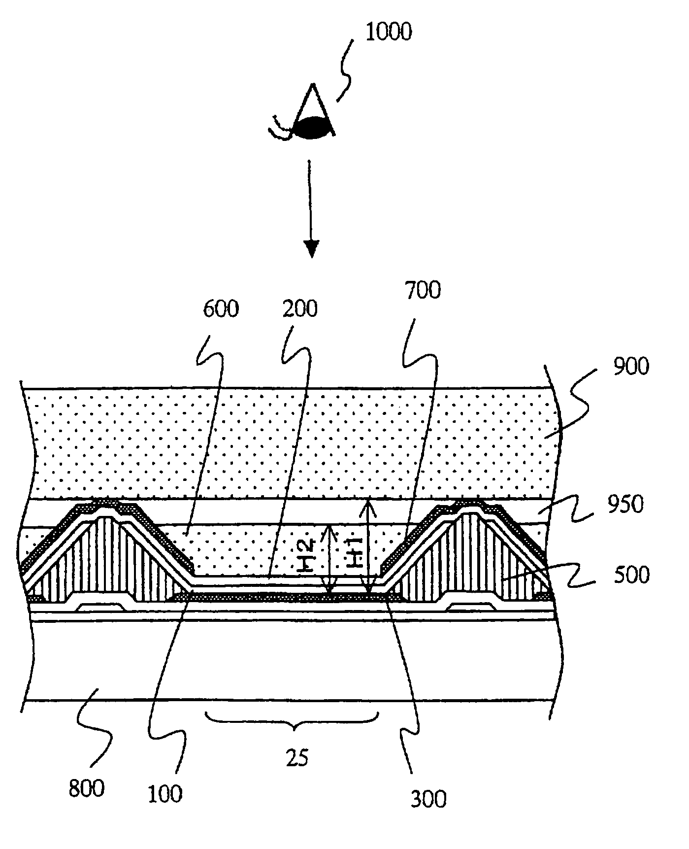
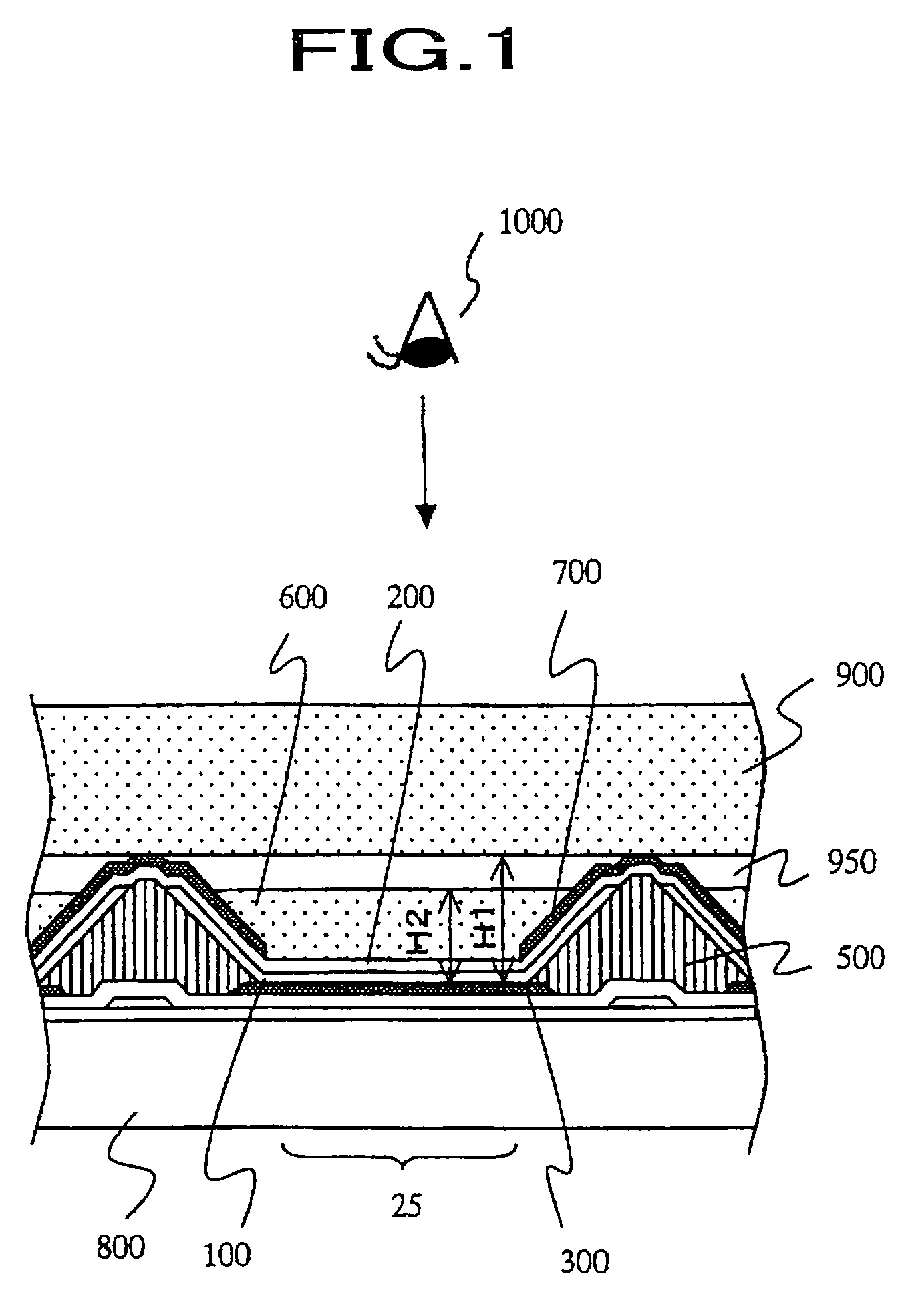
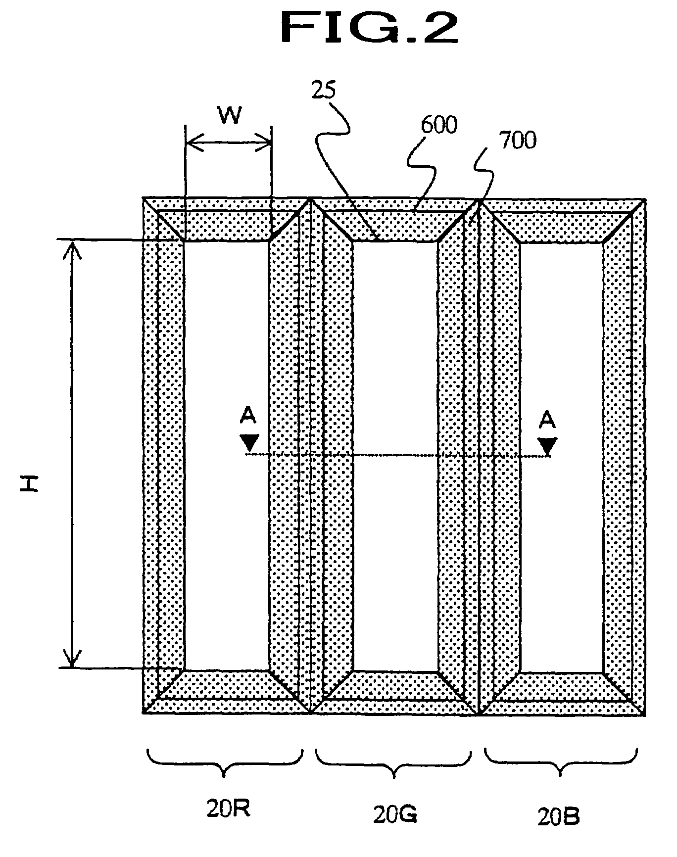
[0049]FIG. 1 shows the cross sectional view of one picture element explaining the first embodiment of this invention. FIG. 2 shows another drawing explaining the first embodiment. FIG. 1 corresponds to the cutaway view along the line of A—A in FIG. 2. One color picture element consists of three picture elements of red-light-emitting picture element 20R, green-light-emitting picture element 20G and blue-light-emitting picture element 20B which are arranged in side-by-side as shown in FIG. 2 and the predetermined color is presented by additive color mixing of the lights emitted from these three picture elements. In addition, these picture elements 20R, 20G and 20B are called as unit picture elements or sub-pixels and a unit picture element corresponds to a mono-chromatic picture element for the case of mono-chromatic display device.

[0050]For the display device according to the present invention, wires, switching elements, storage capacitors and insulating layers fo...

second embodiment

The Second Embodiment

[0104]Next, we will explain another embodiment of the display device regarding to this invention. FIG. 17 shows a cross sectional view of another embodiment of the display device. In this display device, the height H3 of the optical waveguide layer locating at the central area of the basin area surrounded by the bank 500 is continuously larger as being closer to the bank 500. Besides the height H4 of the optical waveguide layer 600 on the tilted reflective surface 700 is larger than H3, we will use the same signs and notations for the same portions and omit the detailed explanation.

[0105]For the optical waveguide layer 600 which satisfies the relation of these heights, we can form it by controlling the dry out speed of the coated optical waveguide layer compound material when we coat the optical waveguide layer compound consisting of binder resin and solvent with taking the boiling point and the vapor pressure of the solvent in the room temperature into account....

third embodiment

The Third Embodiment

[0108]Next, we will further explain another embodiment of the display device regarding to this invention. FIG. 20 shows a cross sectional view of a picture element in this another embodiment. For this embodiment of the display device, the thickness of the optical waveguide layer has the maximum at the center of the area surrounded by the bank 500 and is continuously less as being closer to the bank. Since the fundamental construction is same as the embodiment described above besides the shape of the optical waveguide layer is convex, we mark with the same signs and notations to the same portions and avoid the explanation. This shape of the optical waveguide layer is made by making the tilted reflective surface 700 liquid-repellent and the transparent electrode 200 exposing to the optical waveguide layer liquid-wettable before coating the optical waveguide layer compound material consisting of binder resin and solvent. As a concrete process, the substrate is expos...


PUM


Abstract

A self light emitting display device having high level of the external coupling efficiency and high grade image presentation as no optical cross-talk or blur can be obtained by a new light-emitting element. The device is constructed as follows. A plurality of picture elements, each of which picture elements has an organic layer composing light emitting areas, a transparent electrode and a reflective electrodes, are formed on a substrate. Between the picture elements, a bank which has a tilted reflective surface is formed so that the light emitting area is surrounded by the bank wherein the transparent optical waveguide layer is formed as optically isolated for each of the picture elements.

Description

FIELD OF THE INVENTION[0001]The present invention relates to a light-emitting element and a display device that presents picture images by controlling the light-emission operation of the light-emitting element, especially, to a technology that can be effective to such a light-emitting element as an organic light-emitting diode and to a display device equipped with the organic light-emitting diode.BACKGROUND OF THE INVENTION[0002]An organic light-emitting diode (abbreviated as OLED hereinafter) is a device that converts electric energy to light energy by injecting hole and electron to a light-emitting layer constructed with an organic thin layer. A display device constructed with OLED (abbreviated as OLED display, hereinafter) features the thinness and lightness because no additional light as backlight is required due to the self light-emitting capability. Furthermore, OLED display has other features as wide viewing angle and quick time-response in display characteristics.[0003]FIG. ...

Claims


Application Information

Patent Timeline
Patent Type & Authority Patents(United States)
IPC IPC(8): H05B33/00H05B33/22H05B33/02H01L27/32H01L51/52H05B33/04H05B33/12H05B33/26
CPCH01L51/5275H05B33/04H05B33/14H05B33/02H01L51/5271H01L27/3246H01L51/524H05B33/22H01L51/5203H01L27/3211H01L51/5281H01L27/322H01L27/3248H01L51/5206H01L51/5237H01L51/5221H01L27/3295H01L2251/5315H10K59/35H10K59/38H10K59/122H10K59/123H10K50/81H10K50/828H10K50/841H10K50/8426H10K50/8428H10K50/856H10K50/86H10K2102/3026H10K2102/321H10K50/84H10K50/85H10K50/805H10K50/858H10K59/124H10K59/1213H10K59/1216H10K50/82
Inventor ADACHI, MASAYATSUJI, KAZUTAKAMURAKAMI, HAJIMENISHIMURA, ETSUKO
Owner SAMSUNG DISPLAY CO LTD
Why Eureka
Try Eureka