Grating coupler and application thereof in polarization and wave length beam splitting

A grating coupler, grating coupling technology, applied in the coupling of optical waveguides, diffraction gratings and other directions, can solve the problems of low coupling efficiency, inability to solve the huge difference in thickness, long-term alignment work, etc., to achieve the effect of high coupling efficiency

Active Publication Date: 2009-10-14
PEKING UNIV
View PDF0 Cites 54 Cited by
  • Summary
  • Abstract
  • Description
  • Claims
  • Application Information

AI Technical Summary

Problems solved by technology

This method still cannot account for large differences in thickness, and the coupling efficiency is very low
Moreover, the coupling is very sensitive to vibration and changes in the height direction, requiring good environmental conditions and long-term alignment work

Method used


Image

  • Grating coupler and application thereof in polarization and wave length beam splitting
  • Grating coupler and application thereof in polarization and wave length beam splitting
  • Grating coupler and application thereof in polarization and wave length beam splitting

Examples


Embodiment Construction

[0030] The specific implementation manners of the present invention will be further described in detail below in conjunction with the accompanying drawings and embodiments. The following examples are used to illustrate the present invention, but are not intended to limit the scope of the present invention.

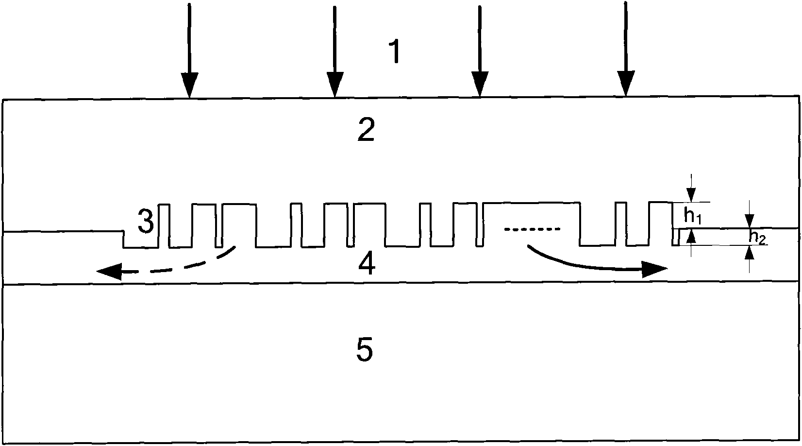
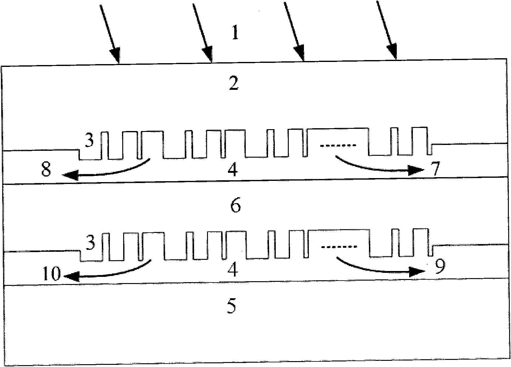
[0031] The invention provides a binary blazed grating coupler, the structure of which mainly includes a waveguide upper cladding layer, a grating layer, a waveguide layer and a lower cladding layer (also called a substrate layer). The output light from the fiber or semiconductor laser enters the surface of the grating from the upper cladding (or lower cladding), and the light is coupled into the optical waveguide below the grating under the action of grating diffraction.

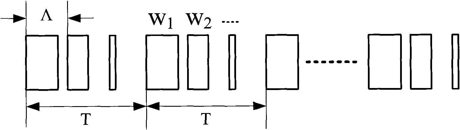
[0032] The blazed grating can blaze the diffracted light to a certain diffraction order, which greatly improves the diffraction efficiency of the grating. The binary blazed grating is a sub-wavelength g...


PUM


Abstract

The invention discloses a grating coupler, which sequentially comprises an upper cladding, a grating layer, a wave guide layer and a lower cladding from top to bottom. The grating layer adopts a binary blazed grating that is a one-dimension binary blazed grating or a two-dimension binary blazed grating. The binary blazed grating coupler provided by the invention can obtain high coupling efficiency and realize complete vertical coupling; besides, the preparation is easy. By adjusting a grating parameter, the grating coupler realizes that incident light is respectively coupled in different wave guides according to different polarization states or wave lengths, thus offering effective ways for polarization beam splitting, wavelength division multiplex, etc.

Description

technical field [0001] The invention relates to the fields of optical communication and optical interconnection, in particular to a coupling structure of an optical waveguide. Background technique [0002] With the development of optoelectronic technology, the size of optoelectronic devices is getting smaller and smaller, especially the development of silicon-based optoelectronics, more optoelectronic functional devices are integrated on the same chip. But at the same time, the small size also brings great difficulties to the coupling and alignment of the system. Generally speaking, the cross-sectional size of SOI (silicon on insulator) integrated optical waveguide is dozens of times smaller than that of ordinary single-mode optical fiber, and even tapered optical fiber cannot overcome such a huge mode field mismatch. The direct end-to-end coupling loss between the single-mode fiber and the single-mode SOI nanowaveguide is greater than 26dB, which is unacceptable to us. At...

Claims


Application Information

Patent Timeline
Patent Type & Authority Applications(China)
IPC IPC(8): G02B6/34G02B5/18
Inventor 周治平冯俊波
Owner PEKING UNIV
Why Eureka
Try Eureka