Composite materials containing carbon nanoparticles

a technology of carbon nanoparticles and composite materials, which is applied in the direction of non-conductive materials with dispersed conductive materials, prosthesis, fullerenes, etc., can solve the problems of brittleness of materials, adversely affecting the properties of materials, and stress within formed materials

Inactive Publication Date: 2006-07-13
CINVENTION AG
View PDF99 Cites 79 Cited by
  • Summary
  • Abstract
  • Description
  • Claims
  • Application Information

AI Technical Summary

Benefits of technology

[0008] One object of the present invention is to provide a process for the production of composite materials that allows for the “tailori...

Problems solved by technology

Disadvantages of common ceramics are the brittleness of the material as one of the problems in connection with their forming process into stable two or three-dimensional structures.
In addition, different thermal extension coefficients of the (different) raw materials might lead to stress within the formed materials if components of the ceramic materials are e.g. applied together with metallic components.
If ...

Method used


Image

  • Composite materials containing carbon nanoparticles
  • Composite materials containing carbon nanoparticles
  • Composite materials containing carbon nanoparticles

Examples


example 1

Modification of the Carbon-Based Nanoparticle

[0101] 1 g of a fullerene mixture of C60 and C70 (Nanom-Mix, FCC, Japan) was mixed together with 99 g of 3-aminopropyl-trimethoxysilane (Dynasylan® AMMO, available from Degussa AG, Germany) in a water bath at 50° C. under continuous stirring (20 rpm) for 20 h to yield a red-brown liquid.

example 2

[0102] 2 g of the above-mentioned silane-modified fullerene liquid mixture was reacted with 0.5 g of TEOS (Dynasil® A, available from Degussa AG, Germany) and 0.5 g of concentrated H2SO4 and stirred (20 rpm) for approximately 4 h at room temperature, resulting in a homogeneous gel. Subsequently, 1.0 g of a phenoxy resin (Beckopox EP 401, UCB Solutia) and 22.5 g of MEK were added to the gel, to yield a dispersion. After applying the dispersion onto glass and steel substrates, the samples were each tempered at 300° C. for 30 minutes. The films were homogeneous, translucent and of yellowish color. The fullerene-containing samples exhibited a surface resistance of 109 Ohms, whereas the polymer film did not reveal any anti-static or conducting resistance. The films were scratch-resistant and elastic, whereby a 90° folding of the coated steel did not show any flaking or cracks within the film.

example 3

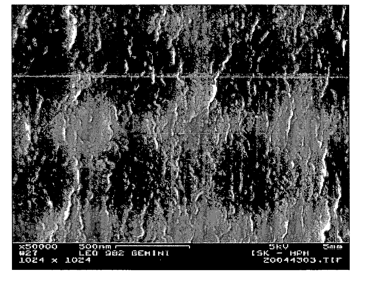
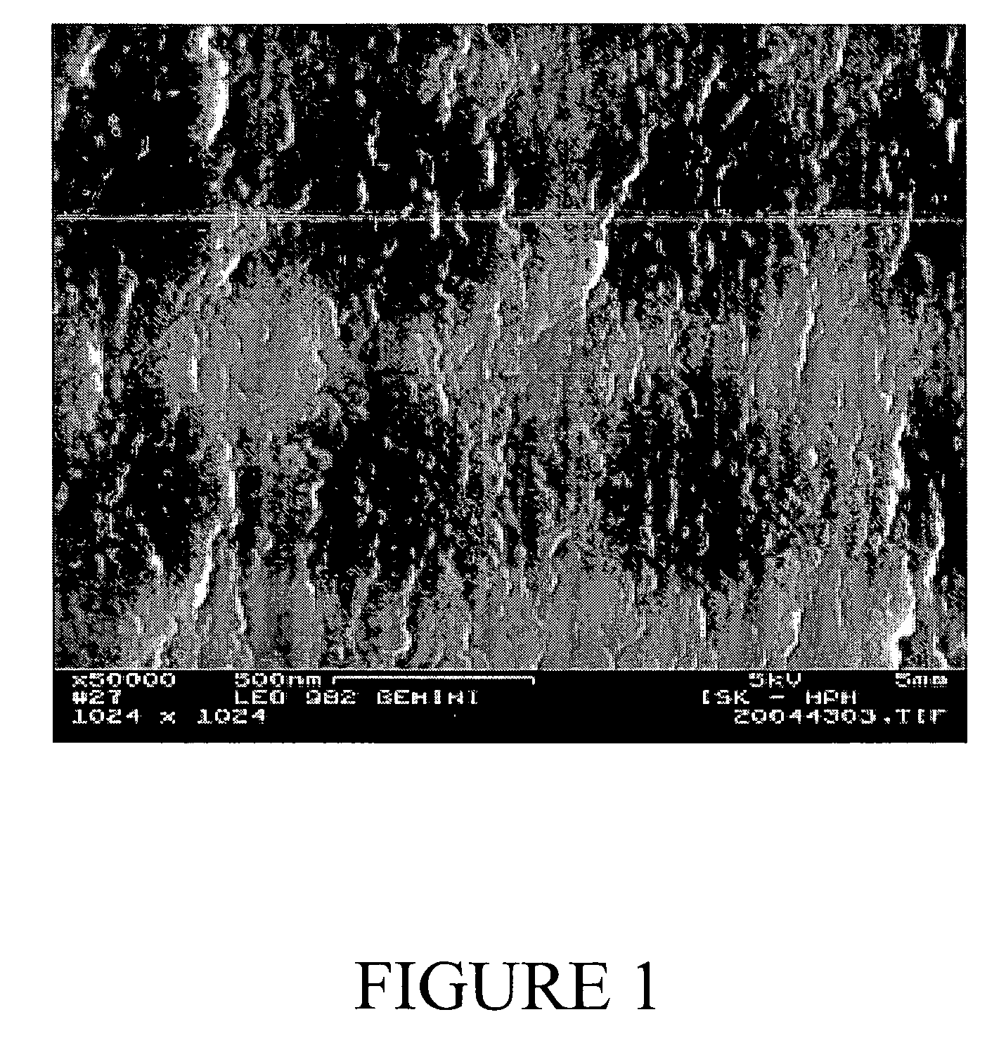
[0103] 4 g of the above-mentioned fullerene mix (Nanom, FCC) was stirred (20 rpm) with 16 g of 2-aminoethyl-3-aminopropyltrimethoxysilane (Dynasylan® DAMO, available from Degussa AG, Germany) at 50° C. for 20 h. 4 g of the resulting liquid mixture containing modified fullerene and residual silane was gelled with 1 g of concentrated HCl, 1 g Tween® 20 (surfactant), 0.5 g of water, and 1.0 g of a phenoxy resin (Beckopox EP 401, UCB Solutia). Thereafter, isophorondiisocyanat was slowly added. The resulting material was cured under ambient conditions at room temperature. FIG. 1 is an SEM picture (magnification 50,000×) of the surface of this gel, which reveals a very uniform distribution of the fullerene particles in the solid gel network.

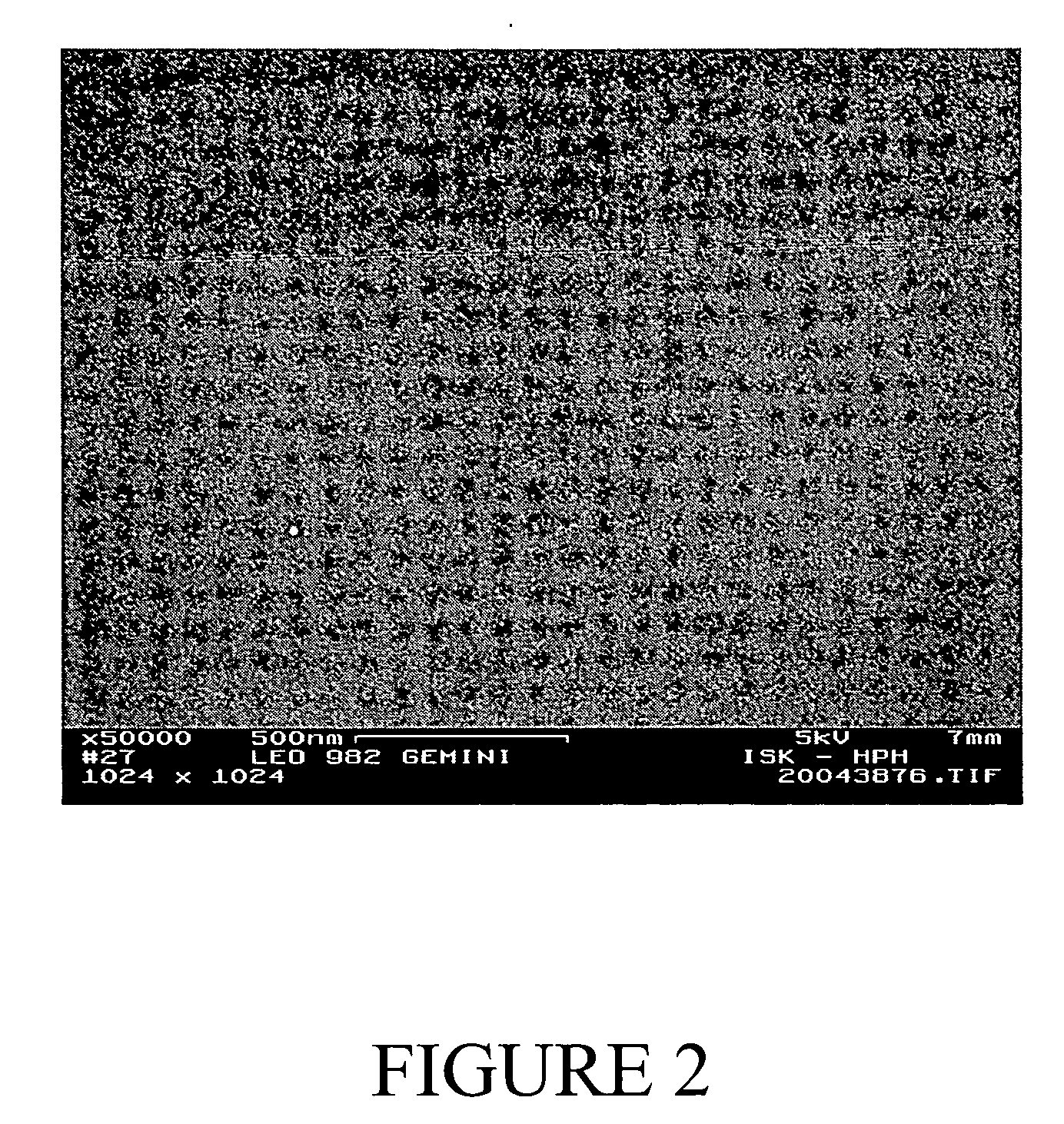
[0104] The solid material was then carbonized oxidatively at 150° C. SEM analysis revealed a porous structure with an average pore size of 1 nm at the surface and cutting edge, as shown in FIG. 2. The specific surface area was revealed to be 4000 m2 / g...


PUM

PropertyMeasurementUnit
Temperatureaaaaaaaaaa
Fractionaaaaaaaaaa

Abstract

The present invention relates to a process of producing composite materials by a sol/gel-process, comprising carbon nanoparticles and organic polymer material. The invention further relates to composite materials, which are manufactured with the use of said sol/gel technology.

Description

CROSS-REFERENCE TO RELATED APPLICATION(S) [0001] This application claims priority from U.S. Patent Application Ser. No. 60 / 643,842, filed Jan. 13, 2005, the entire disclosure of which is incorporated herein by reference.BACKGROUND OF THE INVENTION [0002] Composite materials, in particular ceramics, are used as constructive materials for functionalized components of machines, devices or components and the like that may be exposed to high thermal and mechanical strains because of their mechanical properties and their thermal or chemical stability. In particular, porous ceramics are used increasingly in membranes, filters, catalysts or sensors because of their advantageous properties. In such applications, there is a need for functionalized composite materials, which exhibit certain electrical, di-electrical, magnetic or optic properties or even semi-conducting, ferromagnetic or super-conducing properties. [0003] U.S. Pat. No. 6,255,241 describes a method of producing fullerene dispers...

Claims


Application Information

Patent Timeline
IPC IPC(8): A61F2/28C09D7/62C09D7/65
CPCB82Y30/00C01P2004/03C01P2004/64C01P2006/12C01P2006/16C08J5/005C08K3/04C08K9/04C08K9/06C09C1/56C09D7/1266C09D7/1291C09D7/67C09D7/70H01B1/00C09D7/62C09D7/65C01B32/152B82B3/0009
Inventor ASGARI, SOHEIL
Owner CINVENTION AG
Why Eureka
Try Eureka