Circuit design platform

a technology of circuit design and design platform, applied in the field of circuit design platform, can solve the problem of no service or technology provider that can provide total solutions, and achieve the effect of reducing the time and cost consumed in the design and manufacture of integrated circuits and human resources

Inactive Publication Date: 2006-07-13
WEN KUEI ANN +1
View PDF13 Cites 20 Cited by
  • Summary
  • Abstract
  • Description
  • Claims
  • Application Information

AI Technical Summary

Benefits of technology

[0007] Another objective of this invention is to provide a circuit design platform to integrate all kinds of resources that a circuit designer may use during the d

Problems solved by technology

There is no such service or technology provider that can provide total solutions in helping ci

Method used


Image

  • Circuit design platform
  • Circuit design platform
  • Circuit design platform

Examples


Embodiment Construction

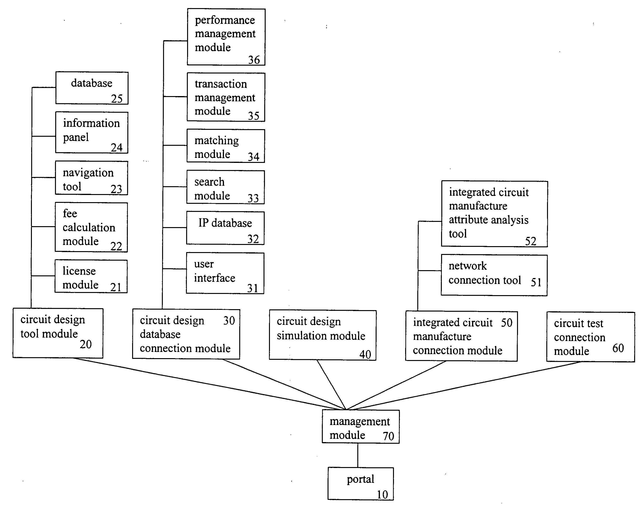
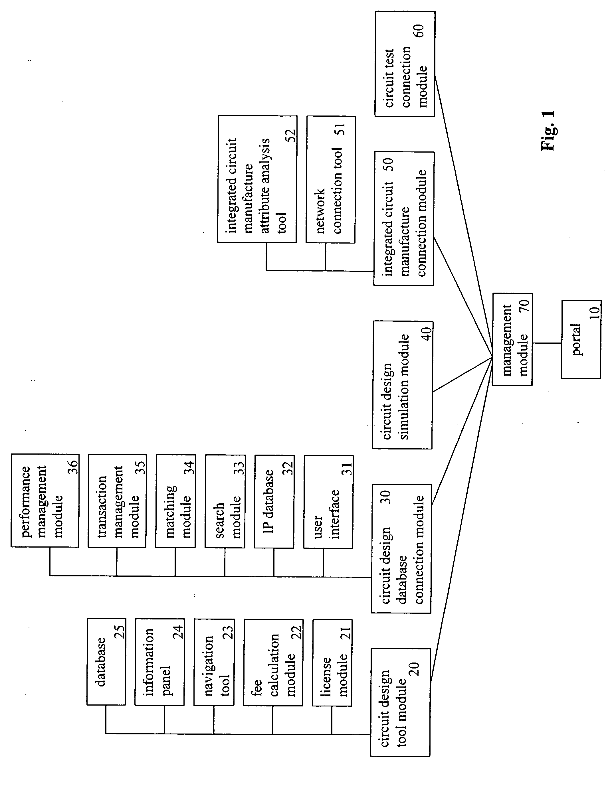
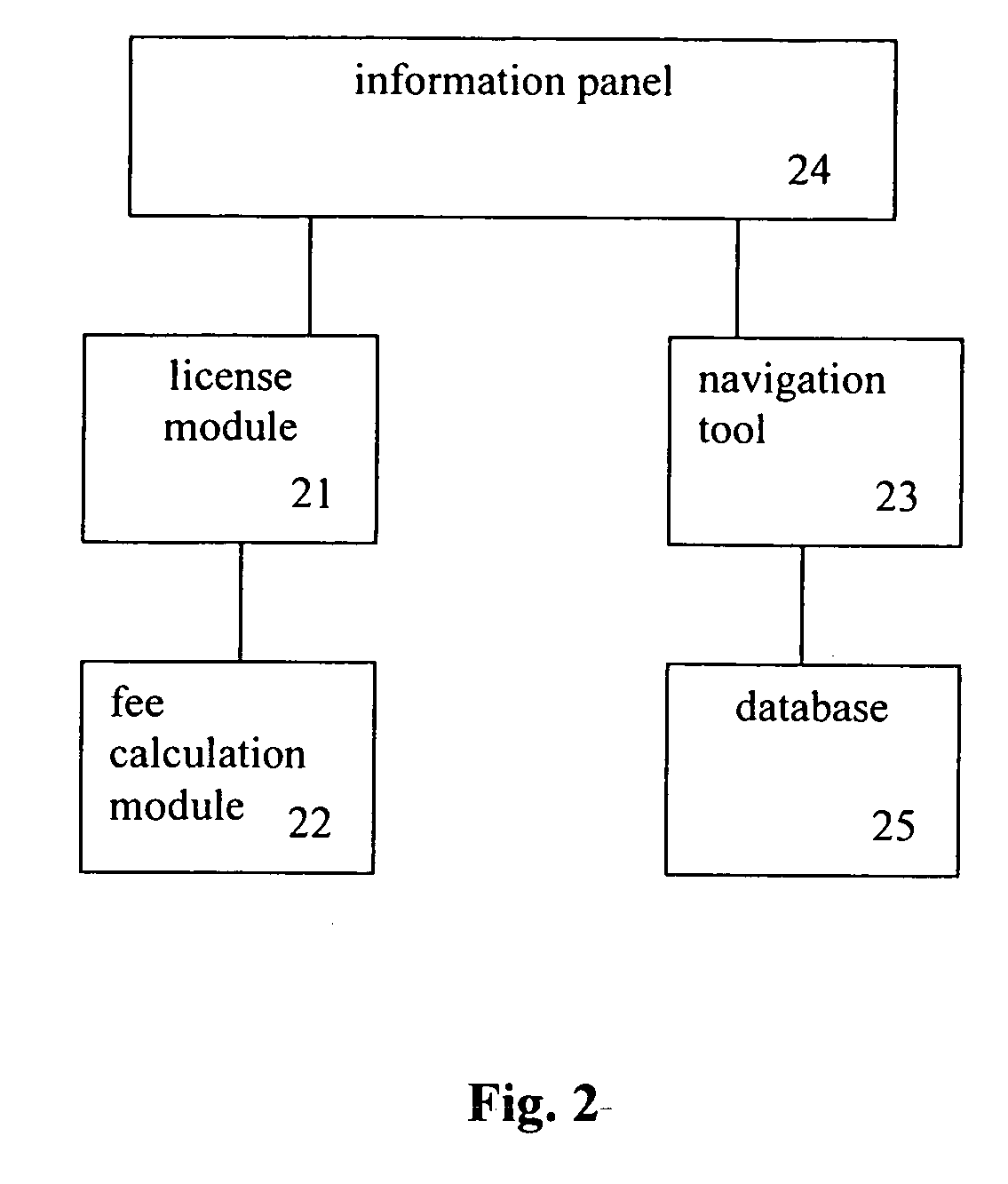
[0020]FIG. 1 shows the systematic diagram of the circuit design platform of this invention. As shown in this figure, the circuit design platform of this invention comprises: a portal 10 to provide a network platform mechanism to be connected to functional modules including the following circuit design tool module 20, circuit design database connection module 30; circuit design simulation module 40, integrated circuit manufacture connection module 50 and circuit test connection module 60. The circuit design platform 10 may further include other functional modules to integrate all necessary functions from design, simulation, manufacture, test, package and other required functions into the platform. The circuit design platform of this invention may further comprises a plurality of software design, simulation, test and even sales, installation and after service tool modules and other database connection modules to allow circuit designers to generate necessary systematic software or appl...


PUM


Abstract

The circuit design platform of this invention comprises: a portal provided with a network platform to install functional modules and to allow users to utilize said functional modules after login; a circuit design tool module to connect at least one circuit design software and to generate a circuit design descriptive data file; a circuit design database connection module to connect at least one circuit design database; a circuit design simulation module to connect at least one circuit design simulation software; an integrated circuit manufacture connection module to connect website of at least one integrated circuit manufacturer and to provide at least one integrated circuit processing attributes analysis tool to suggest suited manufacture process; a circuit test connection module to connect at least one circuit test service provider to conduct online or offline tests; and a management module for management and fee calculation of access of the above functional modules.

Description

FIELD OF THE INVENTION [0001] The present invention relates to a circuit design platform, especially to a system of integrated working platform provided with all kinds of tools allowing circuit designers to analyze, design, simulate, verify and manufacture integrated circuits in the same platform. BACKGROUND OF THE INVENTION [0002] Along with the highly integration of the integrated circuit, to include millions of transistors in one integrated circuit has been a known art. Under such technical trend and such business practice, all steps and aspects involved in the design of integrated circuit shall be assisted by professionals using professional tools. The biological environment of the circuit design industry has thus changed. [0003] In other words, in the early days a circuit designer shall be equipped with a semiconductor factory, so that integrated circuits designed by the designer may be verified and manufactured in the semiconductor factory. However, the raise of professional s...

Claims


Application Information

Patent Timeline
IPC IPC(8): G06F17/50
CPCG06F30/327G06F30/33G06F30/3308
Inventor WEN, KUEI-ANNWUEN, WEN-SHEN
Owner WEN KUEI ANN
Why Eureka
Try Eureka